There is increased interest in ReRAM for embedded computing, especially in automotive applications, as more of its known issues are solved. Nevertheless, there is no one-size-fits-all NVM.

Resistive RAM is gaining renewed attention as demand for faster and cheaper non-volatile memory alternatives continues to grow, particularly in applications such as automotive.
Embedded flash has long left designers wishing for better write speeds and lower energy consumption, but as the leading edge of that technology shrunk to 28nm, another problem arose. Manufacturing flash memory at those dimensions can require a dozen or so masks, which increases the cost. On top of that, flash requires a high thermal budget in the front end, and relatively high voltages.
This is where would-be competitors see a potential opening, and they are making a play with ReRAM. A key argument among ReRAM proponents is that some new applications are demanding higher performance and that improved speed is no longer achievable just through scaling flash.
Memory markets with entrenched players traditionally are difficult for newcomers and new technologies to crack, in part because it’s hard to compete on a cost basis against chipmakers that have fully depreciated their fabs and equipment, and in part because the incumbent technology has been proven to work well over time. On top of that, in markets where there is more than one player, companies are constantly innovating to remain competitive. So if these other technologies can gain a solid foothold, it likely will be at the high end of the NOR flash market where there are new opportunities and higher ASPs, rather than in the mainstream markets where NOR is likely to remain viable.
This is especially true in many automotive applications, where cost is a critical factor. “A typical car has something like 20 flash devices,” said Jackson Huang, vice president of marketing at Winbond. “There is flash in 6 to 8 cameras in a car. The instrument cluster uses flash, and so does the infotainment. And MCUs come with some amount of flash built-in. But what’s really driving this market is that in the past couple of years, with the advent of over-the-air images, the amount of flash usage has increased significantly, both in density and in unit shipments. There are typically a minimum of 2 images, and usually 3. You have a default image, in case something goes wrong, and you have the currently running image, and you have the previous image.”
Xi-Wei Lin, director of applications engineering, EDA group at Synopsys, likewise sees a future of multiple choices. “ReRAM can be used as embedded memory for IoT devices or standalone unit in MCU,” he said. “ReRAM is immune to magnetic attack, so it may be useful for applications in special environments or for unique security needs. NVM will continue to be application-specific choices, depending on performance, power, reliability, density, form factor, and cost. There are always tradeoffs to make, and there is no one-size-fit-all solution, in my opinion.”
Market research supports these conclusions. The NOR market is growing at a 14% CAGR and is forecast to reach $1.64 billion by 2028, according to Business Market Insights. ReRAM, meanwhile, will surpass NOR in value over the next few years, growing at a 17.2% CAGR and forecast to reach $2.16 billion by 2030, according to Data Bridge Market Research. Companies remain bullish for all of these memories, particularly in light of heterogeneous integration and the rapidly increasing volume of data.
“Next-generation persistent memories and legacy NOR flash have many benefits, but they exhibit low endurance and poor write performance,” said Jack Guedj, CEO of Numen. “Read performance is also too slow for some applications, and active read power is too high. This means SoC designers pay a heavy penalty in performance and power by either reading/writing directly from these memories or adding a large SRAM memory to buffer resistive RAM.”
ReRAM, which took a hit under HP’s abandoned efforts, has matured in recent years. Incumbents and start-ups worked out the tricky materials science required to produce consistent results, and in academic and corporate research labs, ReRAM has become the memory of choice for neuromorphic AI applications, as demonstrated last year in the NeuRRAM chip, created in an academic partnership between UCSD and Stanford.
Tony Kenyon, UCL professor and CTO of ReRAM start-up Intrinsic, reflected on the efforts to solve fundamental challenges, like stability. “There were a lot of papers out, going back seven or eight years, where groups were either working their way through the periodic table of oxides or they were doping the oxides with different elements, trying a few devices and then moving on to the next one.”
In one of those efforts, IBM chose ReRAM based on hafnium dioxide (HfO2) because of its prior familiarity with the material through its pioneering work on hafnium oxides for logic transistors. IBM is now tweaking it to meet the requirements for deep learning.
Intrinsic has chosen to work with silicon oxide. “We can do something more interesting with the oxide,” Kenyon explained. “We can take what is nominally a very insulating material, a very good dielectric, and by structuring the oxide in particular ways, and not making the very defect-free uniform, flat interface stoichiometric oxide that has been used for decades, but engineering it in a slightly different way, we can take that material and make it switchable. We can vary the resistance between two very distinct states, a high resistance and a low resistance state. Depending on how we program and create the device, it can be many more states as well, and in a sense, even an analog variation of resistance, but for memory devices, for ReRAM memory devices, two states is a good starting point.”
Potential eFlash replacement
ReRAM is now one of the leading contenders to replace the high end of the embedded flash (eFlash) lineup, although not likely NAND flash. As Objective Analysis wrote in its 2023 Emerging Memories report, “Over time, the NOR embedded in most SoCs will be almost entirely replaced by either MRAM, ReRAM, FRAM, or PCM, and this will also help drive the success of stand-alone new-memory chips.”
According to Gary Bronner, senior vice president of Rambus Labs, “Compared to embedded flash, ReRAM requires a smaller number of masks to integrate with a CMOS process, scales to smaller nodes, and is byte addressable. The main metric for conventional NAND flash is cost per bit, and ReRAM is not competitive.”
Another example of ReRAM getting traction is Weebit Nano’s ReRAM now being fully qualified and available in SkyWater Technology’s 130nm CMOS process.
Further, TSMC and Infineon, which have jointly developed ReRAM (also known as RRAM) for years, now incorporate it into automotive microcontrollers.
“Several years ago, we decided RRAM was the right choice for embedded memories as we moved toward advanced process nodes,” said Sandeep Krishnegowda, vice president of marketing and applications at Infineon. “It’s a low-power technology. It’s byte-addressable, so unlike flash, you can do direct writes. The endurance and retention performance are compatible with flash and it’s lower cost. We’ve been collaborating with TSMC for over a decade in developing the technology and algorithms to make RRAM. We started by using RRAM in some of our chip cards, the cards that you use for cashless payments and secure authentication. In the consumer industrial market of controllers and MCUs, we use such memory as an embedded flash replacement. Most recently, we’re bringing it to automotive.”
For chips cards, ReRAM has another advantage in that it is immune to radiation with high electromagnetic tolerance. “If you think about payment cards and how everybody wants to extract information, you want your memory to be very robust,” Krishnegowda noted.
In addition, because ReRAM isn’t charge based, there are no leakage issues, Kenyon said.
ReRAM basics
While the materials science in ReRAM is extremely complicated, the basic theory is relatively simple. Instead of charge, ReRAM uses resistance as the basis for switching.
“Basically, it’s a resistor with a variable resistance and that resistance can be changed by applying a specific voltage, and it can be reset and set again,” explained Mark Dickinson, CEO of Intrinsic.
At the heart of ReRAM operation are conductive filaments, which are formed and separated by two different methods. In OxRAM, a metal oxide material is sandwiched between the two electrodes. When a positive voltage is applied on the top electrode, a conductive filament forms between the two electrodes. The filament consists of oxygen vacancies. When a negative voltage is applied on the bottom electrode, the conductive filament breaks. In effect, ReRAM switches between high and low resistive states. The change in resistance is represented by “0” and “1” in the memory.
In CBRAM, though, a copper or silver metal is injected into the silicon, which forms a conductive bridge or filament between the two electrodes.

Fig.1: How ReRAM works. Source: Adesto Technologies
Most commercial industry work, such as the TSMC-Infineon collaboration, now centers on OxRAM.
“Both are called resistive RAM because both are changing resistance of some memory element, but in terms of physics and chemistry, they’re substantially different,” said Ilan Sever, vice president, research and development at Weebit Nano. “In oxygen vacancy we apply different voltage in, and [in the] opposite direction on a resistive layer, and then a conductive filament is created or dissolved based on the voltage that we apply. In that way, we can put the cell into reset — which is, we dissolve the filament, it’s not conductive anymore, the resistance is high. We call that a zero state or reset.”
Intrinsic’s Kenyon explained further, “We’re changing something in the oxide and we’re creating a filament that bridges the gap between the two electrodes. The devices are really simple capacitive-type structures, just one layer of oxide with an electrode on top. And we can create a filament that is conductive that bridges the two electrodes. That filament is made up of oxygen vacancies. So we’re actually moving some oxygen around in the oxide, creating a filament, and then that takes us from the pristine, really high-resistance state to the low-resistance state. When we reverse the polarity, we move the oxygen back in the other direction and re-oxidize a small portion of the filament, not the whole thing, and then we can go backward and forward between the low-resistance and that high-resistance state many, many times.”
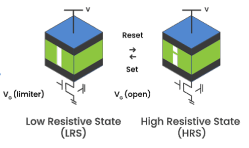
Fig. 2: ReRAM resistance. Source: Weebit Nano
ReRAM disadvantages
Like all memory technologies, ReRAM has its vulnerabilities.
“The fundamental challenge for ReRAM is that it’s noisier than other material options,” said Takashi Ando, principal research scientist at IBM. “In oxide ReRAM, we are moving the oxygen vacancy in a random way. In CBRAM, we are using a cation in a random way. There is some randomness associated with the operation of the device, and that comes with high noise, so the intrinsic noise level is the biggest challenge, but the immunity to the external stimulus is more robust compared to MRAM, or other memory.”
The impact of that noise should not underestimated. “The biggest issue with ReRAM is its intrinsic variability (noise) at a single cell level,” said Synopsys’ Lin. “The resistance variation from one switch cycle to another may be as great as that of a cell population. For filamentary switch-based ReRAM, such as OxRAM and CBRAM, the resistance value is controlled by a small number of oxygen vacancies or metal atoms that move around the filament tip under high electric field and/or high local temperature. The process is fundamentally stochastic in nature, and a few atoms or vacancies can make a big difference. So the noise is intrinsic. Increasing switching currents may mitigate variability to some extent, but at the expense of power consumption.”
Intrinsic’s Kenyon downplays this effect. “The traditional industry view has been that ReRAM has a variability problem because it’s just inherent in the process of creating these filaments and there’s nothing you can do about it,” he said. “But it really comes down to materials engineering questions. We’ve demonstrated that by engineering the material in the right way, you can reduce the variability of the programming voltage, for example, the spread of different voltages required to go from high to low resistance states.”
Takeo Tomine, Totem product manager at Ansys, also pointed out that heat is an issue with ReRAM. “Typically, for advanced technology nodes lower than 7nm, the device size shrinks while supply voltage (Vdd) has been constant — resulting in higher power density and greater metal density, which produce more heat. The self-heating effect is a critical factor influencing the reliability and accuracy of ReRAM. Self-heating becomes most severe where heat is trapped in the transistor device. For ReRAM, temperature variations decrease the Ron/Roff ratio, which is bad for accuracy and reliability in many applications, including AI processing. Careful thermal management is a must, especially in designs with uneven power consumption across different devices. And then, the spreading of this generated heat to nearby layers and devices must be modeled to capture the full-chip heat picture as it evolves over time.”
Lin added a final caveat, “One major challenge to ReRAM technology is the lack of quantitative physical models to a multi-physics, i.e., electro-thermal-chemical problem. Empirical models do exist, but lack fundamental physics. Without good models, it’s difficult to control or optimize manufacturing processes.
Conclusion
ReRAM’s competitors aren’t giving up without a fight. “ReRAM-type technologies write times are quite slow, somewhere around 20,000 to 30,000 nanoseconds. SRAM is like 1 or 2 nanoseconds,” said Numen’s Guedj. He claims Numen’s latest technology can bring ReRAM write time down by 100x, or alternatively, Numen’s MRAM can reduce it further to around 50ns, though the challenge with MRAM is higher processing cost. “There is a need for more technology advancement. Flash cannot scale down. For MRAM, the challenge is to reduce the processing cost, which can happen over time. Most big foundries will keep their options open, try both sides, and hedge their bets.”
Others see the win going to ReRAM. “ReRAM offers two main benefits over MRAM — process simplicity and a wider read window,” said Jongsin Yun, memory technologist at Siemens EDA. “MRAM requires more than 10 layers of stacks, all required to be controlled very precisely to form a matched crystallin. This is challenging to maintain high yield. In comparison, ReRAM has a much simpler stack of layers, requiring relatively less effort to maintain yield. Additionally, MRAM has a very narrow read window (on/off ratio), making it very susceptible to fail by small resistance offsets. On the other hand, ReRAM has more than an order higher read window, making it less susceptible to parasitic resistance offset.”
However in one significant area, MRAM has the lead, so it’s unlikely ReRAM will be a suitable choice for last-level cache. Yun said, “The typical speed of ReRAM falls in the range of microseconds to hundreds of nanoseconds, which is not suitable to use as last-level cache (LLC). As for endurance, ReRAM products typically target endurance around 1E5 [100,000 cycles of write], far less than LLC requirement (1E12 cycles). Due to those limitations, there’s more discussion around MRAM for last-level cache. Adesto, later acquired by Dialog Semiconductor (which in turn was bought by Renesas), demonstrated ReRAM write speeds up to 10ns. In contrast, the IBM and Samsung joint group demonstrated Mbit of MRAM in 250ps, indicating a significant speed difference.”
For this and other reasons, there likely will be several choices of NVMs for the foreseeable future.
“It’s more natural to have NVM suited for each application to become the standard instead of one dream memory applicable to all,” IBM’s Ando said. “My expectation is that we see NVM customized for each application, and that’s already happening for inference and training.”
Finally, Rambus’ Bronner said both MRAM and ReRAM seem to be getting traction as embedded memory. “Broadly speaking, MRAM seems to be slightly higher performance but also higher cost. ReRAM is cheaper, but may not meet the same performance and reliability. Each should be able to find a home, depending upon the tradeoffs that end customers are willing to make.”
References
Related Reading
Resistive RAM (ReRAM/RRAM) Knowledge Center
MRAM Getting More Attention At Smallest Nodes
Why this 25-year-old technology may be the memory of choice for leading edge designs and in automotive applications.
 |
|
 |
 |
 |  |
 |  |
Leave a Reply