Open-source tomography; 4D metrology; new mass spectrometry.

Open-source tomography software
The University of Michigan, Cornell University and Kitware have developed an open-source software platform that enables three-dimensional imaging of nanomaterials.
The open-source platform, dubbed Tomviz 1.0, enables researchers to image and process nanomaterials using electron tomography. Researchers can download the software. Using tomography, the software aligns, reconstructs and analyzes three-dimensional data through a fast pipeline. Tomography is a technique for imaging an object using X-rays or ultrasound.
Traditionally, researchers use proprietary software to handle these tasks with tomography, which is expensive and time-consuming. Tomviz simplifies the process, however. The technology reduces the time, money and computational power required for tomography. It also enables researchers to collaborate and share their findings.
Using hardware-accelerated rendering techniques, Tomviz provides several capabilities. It enables researchers to alter visualization parameters. This includes the ability to alter the opacity, lighting, color and orientation of volumes and geometries of an image. In addition, Tomviz contains multiple tools for analysis.

A 3D view of a particle used in a hydrogen fuel cell. It is made possible by Tomviz 1.0. (Image credit: Elliot Padget, Cornell University)
The software can be downloaded as open-source binaries for Windows, macOS and Linux. Tomviz imports projection images from transmission electron microscopes in standard file formats such as Tagged Image File Format (TIFF), Medical Research Council (MRC) and Electron Microscopy Datasets (EMD).
“We created a responsive, graphical solution that processes and analyzes complex scientific data in a manner that may otherwise span multiple applications and programming environments,” said Marcus Hanwell, a technical leader at Kitware, an open-source software firm, on the company’s Web site.
On the university’s Web site, Robert Hovden, an assistant professor at the University of Michigan, added: “3-D nanoscale imagery is useful in a variety of fields, including the auto industry, semiconductors and even geology. Now you don’t have to be a tomography expert to work with these images in a meaningful way.”
4D metrology
Cornell University has put a new twist on scanning transmission electron microscopy (STEM). Researchers have developed a new type of detector for STEM, enabling a “four-dimensional” map of nanomaterials and tiny structures.
Cornell has licensed the detector technology to FEI, a division of Thermo Fisher Scientific.
A STEM shoots a beam of electrons through a sample. The electrons move back and forth. In the system, a detector looks at the electrons and creates a signal. The signal enables a three-dimensional image on a screen at nano-scale dimensions.
Seeking to improve the STEM, Cornell has devised a new detector, dubbed the electron microscope pixel array detector (EMPAD). The EMPAD can replace the traditional detector in a STEM. EMPAD has a 128 x 128 array of pixels, which are 150 microns each. The array is bonded to a chip that reads out the signals. The EMPAD is part of a work that researchers built for an X-ray crystallography system.
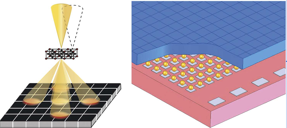
A STEM (left) fires a narrow beam of electrons through a sample. The EMPAD (right) reads the landing point from the scattering angle of each electron. (Source: Cornell)
The detector works in a similar way to image the atomic structures of a sample. The EMPAD-based STEM system builds a “four-dimensional” map, representing the position of electrons as they pass through a sample. The system reveals the atomic structures of a sample. “The EMPAD records an image frame in less than a millisecond and can detect from one to a million primary electrons per pixel, per image frame,” said David Muller, professor of applied and engineering physics at Cornell, on the university’s Web site. “This is 1,000 times the dynamic range, and 100 times the speed of conventional electron image sensors.”
New mass spectrometry
A group that is part of the Chinese Academy of Sciences has developed a new technology called dipolar proton transfer reaction mass spectrometry (DP-PTR-MS).
Using detection techniques based on positive and negative ions, the technology improves identification of organic compounds.
Traditionally, researchers have used proton transfer reaction mass spectrometry (PTR-MS). This provides real-time monitoring of trace volatile organic compounds (VOCs). Recently, a new technology called proton extraction reaction mass spectrometry (PER-MS) has emerged. It can be used for the detection of organic and inorganic compounds.
The Chinese Academy of Sciences combined the functions of PTR-MS and PER-MS in one instrument. This technology, dubbed DP-PTR-MS, can not only detect organic and inorganic compounds, but it enables a more powerful analytical ability to identify VOCs.
Related Stories
Manufacturing Research Bits: March 28
Dental implants; multi-parameter microscopes; ptychography.
China: Fab Boom or Bust?
A frenzy of activity is causing lots of speculation about how this complex market will evolve.
The Week In Review: Manufacturing; March 31
New node metrics; DDR5 standard; fab tool service awards; IC forecasts.
 |
 |
 |
|
 |
 |
 | |
Leave a Reply