Clocks are power- and area- hungry, and difficult to distribute in a controlled manner. What is being done to reign in these unwieldy beasts?

The synchronous digital design paradigm has enabled us to design circuits that are well controlled, but that is only true if the clocks themselves are well controlled.
While overdesign techniques ensured that to be the case in early ASIC development, designs today cannot afford such luxuries. As we strive for lower power and higher operating frequencies, the clock has become a critical design element. Even using modern design techniques, the clock network can consume a significant portion of the routing resources and account for 30% to 40% of total design power.
In the early days of ASIC development, a lot of assumptions and simplifications were made. Delays were on gates, power supplies were totally stable and un-switched, and clocks were perfectly distributed. Many of these assumptions are reflected in the design languages that we use today, such as Verilog and VHDL, and design files have to be supplemented with additional data that includes information such as power intent and post-layout timing.
Other information is left for a tool to extract. Clock tree synthesis (CTS) is one of those areas that has become a lot more complex. Today it relies on a combination of design methodology, tools, manual intervention, and lots of information being passed between different groups within the front-end and back-end teams.
“Design teams spend significant amounts of time during the project to design a clock tree that meets the timing and power criteria of the design,” says Arvind Narayanan, product marketing architect for Mentor, a Siemens Business. “The clock tree complexity is directly dependent on the design architecture and end application.”
Not all designs have the same level of clock complexity. “First and foremost, the number of clocks influences clock tree design,” points out Chuck Alpert, software engineering group director in the Digital & Signoff Group at Cadence. “Some designs have hundreds of clocks and all kinds of skew constraints. Other designs have only a scan and functional clock. Second, the performance targets are a huge factor. Loose skew and transition (slew) constraints enable a more power-efficient clock. Beyond that, other factors include the characteristics of the technology node, floorplan characteristics, and cell library behavior.”
Adding automation
Clock skew has always been a problem for complex designs. “Custom or semi-custom processor design had millions of gates all on the same clock, so they had problems with skew,” says Drew Wingard, chief technology officer at Sonics. “Without solutions that were overkill, it would have been a disaster. They used structured techniques such as putting the clock down right after the power rails and they would lay down structured H trees or gridded clocks.”
Clock tree synthesis was developed to avoid such overkill. Several generations of products have been created to deal with an incrementally increasing problem. Early tools assumed a single clock and as soon as clock gating became a popular way to save power, the tools had to be able to handle multiple sub-trees. Over time, those sub-trees became hierarchical.
One of the difficulties with clocks is their position within the flow. They are neither front-end, nor back-end. Instead, they sit in the divide. “Timing, skew and area can be addressed during implementation, but designing a power efficient clock tree requires the efforts to start early at RTL,” points out Arti Dwivedi, principal technical product manager for ANSYS.
In most cases, the RTL netlist that gets handed off doesn’t model clock skew, although today, skew budgets may be established before running physical synthesis. “CTS has to achieve a skew budget, hopefully at minimum power, and it does that by speeding up some nodes by over-driving them, or it can add delay into other paths,” explains Wingard. “It is easier to slow the clock down than speed it up. As you try and balance a low skew clock over larger distances, the number of buffers in series grows. That means the delay from the source at the top of the tree to when it gets to the leaves, named the insertion delay, grows. The smaller the skew budget, the deeper the clock tree tends to be.”
Alpert asserts that “building a clock tree is essentially a mini physical synthesis (P&R) flow. One must place the clock cells intelligently, optimize the cell sizes and net buffering, time the clock, extract the wires, and route the clock nets. So, the scope of algorithms used in clock tree synthesis spans huge swaths of physical design.”
Mentor’s Narayanan points out this is a multi-level problem. “Since the leaf clusters (wire and pins) carry most capacitance in the clock tree, having dynamically updated RC calculation during CTS allows for leaf clustering that minimizes capacitance, and therefore reduces power. The CTS tool should also work on-the-fly with the global routing engine, during clock buffer insertion so that the CTS engine sees more accurate topology and congestion.”
Managing skew
Skew has to be managed, not necessarily minimized from source. “CTS engines usually aim for zero skew by balancing the signal arrival time across all the flops regardless of which level of the clock tree they inhabit,” says Narayanan. “However, not all clock end points need to be balanced with each other. These different groups have different clock end points, better known as ‘skew groups.’”
In many cases, a CTS tool can analyze flop interactions to derive the skew balancing requirements at the different clock tree levels, and also across different voltage islands. Tools also can discover skew groups by analyzing connected components in the timing data structure. “Using skew groups saves processing time by eliminating manual CTS specifications and multiple CTS runs,” adds Narayanan. “And it also saves power by reducing the number of buffers inserted.”
Clock gating
The clock is a high-activity node that switches twice as fast as most data. “At smaller technology nodes, the clock network is responsible for about half the power consumed on any chip and the majority of it is dynamic power due to the toggling clock,” points out Narayanan. “Both conventional clock trees and mesh based (H-Tree or Fishbone) clock trees can consume significant die area with the big drivers and repeaters in the clock tree to the meet the tight balancing requirements. Clock gating used to optimize power also has a direct impact on area.”
Clock gating reduces clock power by shutting off the clock to unused blocks, but has to be done with care. “Synthesis clock gating alone may lead to insertion of too many clock gates which themselves may burn quite a lot of power,” points out Dwivedi. “RTL techniques can quantify power savings upfront and qualify which clock gates will save power.”
It is also important to consider where the clock gating is performed. “You want to do multiple layers of clock tree gating,” says Wingard. “Close to the registers is good for making local decisions, which can happen very fast, but other times you want something associated with an IP block so that you can remove the local clock to that block. There are times when you want something even higher level, perhaps at the sub-system level or back at the clock generation unit. The closer you gate to the source then the more you can reduce dynamic power.”
Dwivedi agrees. “Designers can get a better control on clock power and timing closure using a combination of coarse and fine clock gating. Block-level clock gates are inserted to turn off clocking in blocks which are not expected to be active during a specific mode of operation. Coarse clock gating can be implemented in one or two stages to ensure efficient clock gating of large blocks or register banks. RTL techniques can identify such scenarios.”
All of this leads to additional complexity. “With the proliferation of mobile devices, clock trees have become extremely complex circuits with different clock tracing per circuit mode of operation,” says Narayanan. “Building robust clock trees that can withstand process variation is a huge challenge for the design teams.”
The growth in the number of operating modes, process corners and power states coupled with the large variation of resistance seen across various process corners require designers to adopt smarter methods for CTS and clock optimization. “Specifically, to lower power in clocks trees, the CTS engine must handle MCMM scenarios and use advanced techniques like intelligent clock gating, skew groups, and slew shaping,” adds Narayanan. “With power-aware CTS optimization, the designer can achieve the best QoR for both power and timing without sacrificing area, or time to closure.”
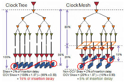
Figure 1: Managing skew with on chip variation. Courtesy of Synopsys
Too much of a good thing
It might appear that keeping the clocks low-skew across the chip is a good thing. Actually, that can lead to problems. “Simultaneous switching of clock gates can lead to high peak power and high di/dt which can stress the power distribution networks,” says Dwivedi. “This is also important for test modes. Early cycle-based power analysis at RTL can help designers identify such critical vectors for dynamic voltage drop analysis.”
To reduce those peaks, the clock arrival time can be skewed on purpose. “If you skew the clock signal to arrive at different cells at different times, you can distribute the power usage uniformly over the clock period,” says , CEO for Teklatech. “As a result, the peak power for the entire circuit is reduced to substantially the peak power of a single cell.”
Another way to reduce power is to make the clock edges less perfect. “Slew is the clock transition, or how long it takes for the clock to switch,” explains Narayanan. “Slower slew means slower timing and lower power, while faster transitions draw more power but can improve timing and signal integrity. Slew shaping is the ability to eliminate transitions that are overly pessimistic to reduce dynamic power while at the same time meeting the timing constraints.”
Clocks in FPGAs
A discussion about clocks would not be complete without at least a mention of clocking within FPGAs. FPGAs have fixed wiring, fixed-size buffers and many other restrictions. Luckily, all of the delays are known up-front.
Jarrod Thorne, senior product line manager for timing and synchronization at Microsemi, points to some of the items that are important in clock tree generation. “The number of inputs and outputs is the primary driver in the complexity of the clock tree solution and the number of devices required. Frequency families impact the complexity of the eventual clock tree solution and you have to ask questions such as, ‘Are all of the clocks required at power-up?’ Using these requirements while constrained by power, cost, board area and number of devices, designers can map to devices to create their clock tree.”
Avoiding the issue
One technique being used increasingly is to avoid the issue at the highest level of design. Fully globally synchronous systems are becoming impractical. Instead, systems are being designed where clocks are treated as if they come from different PLLs. In effect, they are considered to be asynchronous to each other.
However, care needs to be taken at the clock/data domain crossings. “The theory of synchronizer design is dependent upon the fact that the clocks are not synchronized to each other and thus input edges that were sent by the sending clock and clocked by the receiving clock, move relative to each over time,” points out Wingard. “If they are in fact synchronous, you can end up where skew becomes the enemy of the synchronizer. Designs can be bad from a meta-stability aspect because two things that were synchronous were treated as asynchronous.”
Conclusions
The clock is not a perfect signal in the way in which it is represented in an RTL model. It is probably the most complex signal in the entire design and influences every aspect of the system from timing closure to peak power demand, and from chip architecture to layout. Most companies have well defined methodologies related to their treatment of the clock and tools have come a long way in detecting what can be done and finding suitable solutions. But at the end of the day, the engineers can never take their eye off the ball—or in this case, the clock edges.
Related Stories
Choosing Power-Saving Techniques
There are so many options that the best ones aren’t always obvious.
Power State Switching Gets Tougher
Understanding and implementing power state switching delays can make or break a design.
The Time Dimension Of Power
Power is a complex multi-dimensional, multi-disciplinary problem. Does your flow address all of the issues?
The Ultimate Shift Left
Many implementation steps have been moving earlier in the design flow. Floorplanning is next, and it encompasses everything from architectural to physical.

 |
|
 |
 |
 |
 |
 |
 |
 |
 |
“Clocks in FPGAs
A discussion about clocks would not be complete without at least a mention of clocking within FPGAs. FPGAs have fixed wiring, fixed-size buffers and many other restrictions. Luckily, all of the delays are known up-front.”
Intel Stratix10 has “registers everywhere” and selects the FF based on in path and out path to allow more time for long paths to resolve.
The next step is to use wiring delay to time clocks to allow for nets to resolve for self clocking rather than synchronous clocking.
This would help make asynchronous design practical.