Technology could play a bigger role in 3D NAND, but control and cost remain problematic.

After years in R&D, a technology called cryogenic etch is re-emerging as a possible option for production as the industry faces new challenges in memory and logic.
Cryogenic etch removes materials in devices with high aspect ratios at cold temperatures, although it has always been a challenging process. Cryogenic etch is difficult to control and it requires specialized cryogenic gases in the fab, which are expensive.
Developed in the 1980s, cryogenic etch has some merits, but it has been primarily used in R&D, and not in production, for MEMS and other devices. The industry doesn’t actually sell cryogenic etch systems. But for years, several tool vendors have sold etch tools with cryogenic capabilities. The purists contend that an etch conducted at a temperature of minus 100°C (minus 148°F) or below constitutes a cryogenic etch.
Cryogenic etch, sometimes called cryo etch, is one of two ways to enable deep silicon or high-aspect ratio (HAR) etches in devices, where the features are long, narrow and deep. The other and most popular method is the two-step Bosch process, where you etch out a part of the structure and then passivate it at ambient temperatures. Then you repeat the process until the etch is completed.
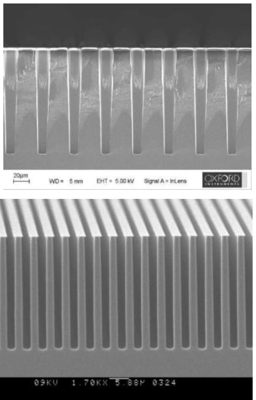
Fig. 1: Cyrogenic etch for high aspect ratios. Source: AZoNano.com/Oxford Instruments Plasma Technology
While the industry will stick with the Bosch process for the most part, some are beginning to look at cryogenic etch for production, at least for a narrow set of applications. In simple terms, cryo etch is a one-step technique that cools the structure during the process, which prevents unwanted reactions that can impact the etch profiles.
The drawback is that cryo etch requires low-temperature chillers or an expensive liquid nitrogen gas line at the point of service in the fab. That’s why the technology has been relegated to R&D.
But as conventional etch problems face challenges, particularly with 3D NAND—the successor to today’s planar NAND flash memory—cryo etch is getting a serious look.
“What we’re doing is introducing cryogenic etching,” said Rick Gottscho, CTO of Lam Research, during a recent presentation. “It’s been in the literature since the mid-1980s, but it was very much ahead of its time. It’s a difficult technology, but we’ve made great progress.”
For years, Oxford Instruments, Plasma-Therm and others have sold etchers with both cryogenic and non-cryogenic capabilities. Now, Lam and others are looking at cryogenic etch for 3D NAND. And the industry is also developing the technology for low-k dielectrics in logic devices.
The Bosch process will remain the dominate technology in production. But cryo etch presents some intriguing options, even if it’s unclear whether the industry can bring it into production.
What is etch?
Etch, the process step that etches or removes materials from the wafer to create the features of a device, is split into two categories—wet and dry. Wet etch uses liquid chemicals to remove materials.
Dry etch is the larger of the two markets. Generally, cryo etch, atomic layer etch (ALE) and other types fit into this category. Cryo etch is different than ALE, however. ALE, which is moving into production, selectively removes targeted materials at the atomic scale.
In many dry etch systems, though, a wafer sits in a reactor in an etch system and plasma is used as the source. Gas is introduced in the system and the plasma breaks up the gas, generating ions and reactive neutral species. Then, the ions and species bombard a select part of the wafer, which removes the materials in the device.
A plasma etch system is configured with one of several types of reactors, such as capacitively coupled plasma (CCP) and inductively coupled plasma (ICP) and others.
An etcher based on a CCP plasma source consists of a reactor and two metal electrodes. The wafer sits on a stage between the two electrodes. Using an RF power supply, an electric field is generated between electrodes, which releases ions.
In the fab, the most advanced etchers are based on ICP. These etchers resemble the CCP system, but the ICP source creates energy via electromagnetic induction.
Both CCP and ICP enable a process called reactive ion etching (RIE). “You have reactive and ion etching. The reactive is our chemical etching. You can think of this as almost a wet acid etch,” explained Geoffrey Gardner, a research associate for Microsoft Research and a visiting scholar at Purdue University.
“Ion etching is much more of a mechanical process. The analogy I would give it is sandblasting. You are mechanically removing something on the surface,” Gardner said. “When I combine these together, I get an advantage. It will increase the rate at which my reactive etching is taking place.”
So RIE is a process where ions bombard the surface, and adding an ICP etch tool allows you to control the process. “When I have inductively coupled plasma, I can now independently tune my plasma density, so I can make it much richer or more potent. Then, with a separate knob, I can control my ion energy,” Gardner said.
An ICP etcher can perform an RIE process for various applications on a device, such as mask etch, HAR etch and others. HAR etch is also known as deep silicon etch or deep reactive ion etch (DRIE).
For HAR etch, the industry mainly uses the Bosch process. Patented in 1996, the two-step process first involves an isotropic etch using sulfur hexafluoride (SF6), followed by a protection film passivation layer. The Bosch process is robust, enabling HAR etches up to 100:1. But at times, the process can result in rough sidewalls and imperfect etch profiles.
Cryo etch, meanwhile, is another way to perform HAR etches. Using an RIE process, cryo etch enables a HAR of >50:1, depending on the process. Some claim it enables 100:1.
For both the Bosch and cryo etch technologies, however, the process becomes less predictable at aspect ratios above 30:1, according to experts.
Regardless, cyro etch has some advantages. Like the Bosch process, cryo etch is conducted in a standard ICP etcher. The same etcher can also accommodate non-cryogenic processes. The key is the wafer table in the etcher. If the table is cooled to cryogenic temperatures in the system, the etcher is performing a cyro etch. If it’s not cooled, it is performing a different etch.
Generally, the etcher may have a chiller attached to it, which can take the temperatures to minus 10°C to 20°C. But in a pure cryo etch process, a liquefied nitrogen gas is pumped into the tool, enabling temperatures below 100°C.
For example, Oxford Instruments sells an ICP etch tool. “Our wafer table has both cooling and heating, and can operate across a wide temperature range (-150°C to +400°C),” said Mike Cooke, CTO of Oxford Instruments Plasma Technology. “It can, in fact, go colder than -150°C, but at lower temperatures, it is more like a cryo pump than a table, freezing many etch gases.”
Unlike the Bosch technology, cryo etch is a continuous process. Generally, SF6 and O2 gases are used in cryo etches. This in turn produces fluorine radicals for etching.
“Applications are mainly deep silicon etch,” Cooke said. “Any process with mixed ion-stimulated etching and a chemical etching occurring at the same time can be tuned by adjusting the wafer temperature.”
It has some advantages over the Bosch process. “Unlike gas-chopping etch/passivation cycles, the sidewall is free of scallops,” he said.
For example, let’s say you want to etch a deep trench. In cryo etch, the ions are removing the materials in the trench until they reach the bottom, but the sidewalls remain at cryogenic temperatures. “I like to think of it as ion-assisted reactive etching. By keeping the substrate cold, only where the ions hit is where it warms up. That heat doesn’t spread out to the rest of the wafer,” Microsoft Research’s Gardner said.
Cryo etch prevents unwanted mishaps during the process. “Atoms move around at high temperatures,” said Mahendra Pakala, managing director of process development at Applied Materials. “If you don’t want the atoms while etching, you reduce the temperatures.”
Still, cryo etch has been stuck in R&D. “It’s pretty much an R&D effort, but it is possible that it has been used in some MEMS work for deep trenches as well as line-edge roughness,” said Dean Freeman, an analyst at Techcet. “The challenges are MFC control, temperature control, humidity control and O2 levels. It also looks like there are some pretty tight process windows.”
What has kept cryo etch in R&D is that it requires a liquid nitrogen gas service. “The cost comes from having to create a dedicated line then insulating it. It’s possible to have a dewar close to the etch tool, but then you have to pay very close attention and change it out as needed, which is an added expense,” Freeman said.
There are some niche-oriented applications for cyro etch, mostly in R&D. “The primary applications for cryo are silicon structures that require roughness of less than about 10nm, very high aspect ratios, and polymer-free or low-volume production of nanostructures,” said David Lishan, principal scientist and business development manager at Plasma-Therm.
“This is often for maximum performance photonic devices, such as waveguide or reflecting surfaces, or microfluidics where turbulence must be at a minimum,” Lishan said. “Another potential application is when nanostructures with careful profile and dimensional control are needed. One example of this is master masks for nanoimprint technology. The other driver for cryo is a polymer-free process. Being polymer-free eliminates the typical post-DRIE polymer removal process step.”
Frozen memory and logic
Now, however, cryogenic etch is inching closer from the lab to the fab. The technology is being evaluated for 3D NAND. Unlike today’s planar NAND, which is a 2D structure, 3D NAND resembles a vertical skyscraper in which horizontal layers of memory cells are stacked and then connected using tiny vertical channels.
3D NAND is quantified by the number of layers stacked in a device. As more layers are added, the bit density increases. Today, 3D NAND suppliers are shipping 64-layer devices with 96-layer products ramping up. And behind the scenes vendors are developing 128- and 256-layer products.
The 3D NAND flow starts with a substrate. Then, using chemical vapor deposition, a layer of material is deposited on the substrate, followed by another layer on top. The process is repeated several times until a given device has the desired number of layers.
Then comes the hardest part of the flow—HAR etch. For this, the etch tool must drill tiny circular channels from the top of the device stack to the bottom substrate.
This step is performed using RIE etchers. The etcher creates tiny channels by bombarding the surface with ions. But as the etch process penetrates deeper into the channels, the number of ions may decrease. This slows down the etch rate. Even worse, unwanted CD variations may occur.
Regardless, today’s etch tools work for up to 64 layers and perhaps 96, but the systems are running into issues beyond that point. “For 9x layers, some use conventional etchers. However, for more HAR etching, another plasma tool/method is needed. Cryogenic etching is an example,” said Jeongdong Choe, an analyst at TechInsights.
In theory, for this application, a cryogenic etcher would drill tiny holes at cold temperatures. This keeps the sidewalls cold during the etch process, which allows the ions to move further down the holes without disruption.
“The advantage of cryogenic etching is that you get more reactants down at the etch front at the bottom of this high aspect ratio feature,” Lam’s Gottscho said. “That enhances the etch rate. That’s an expensive technology to implement, but the benefits outweigh those added costs.”
There are some challenges. “For dielectric layers, such as oxide and nitride, (cryo etch) is still an ongoing development,” TechInsights’ Choe said. “We can get a very vertical etching profile. It’s easy to apply this on a wide open area. However, because of the residue, it’s difficult to get a deep hole etching profile with SiO/SiN alternative dielectric layers on a dense array cell area.”
To be sure, the industry can continue to scale 3D NAND without cryo etch. On the other hand, the technology may make scaling a bit easier, if it works. That’s the big unknown.
Besides 3D NAND, the industry is also looking at cryo etch for logic. A logic chip consists of a transistor and interconnects. The transistor resides on the bottom of the structure and serves as a switch. The interconnects, which reside on the top of the transistor, consist of tiny copper wiring schemes that transfer electrical signals from one transistor to another.
To make the copper interconnects, the industry uses a dual-damascene process. In this flow, a low-k dielectric material is first deposited on the surface of the device. Based on a carbon-doped oxide material, low-k films are used to insulate one part of the device from another and reduce parasitic capacitance.
The next step is to pattern the vias and trenches on the low-k film. The structure is etched, forming a via and trench. Finally, the via/trench structure is filled with copper, creating a copper wiring scheme.
There are several challenges. For example, today’s low-k films have a “k value” of 2.5 or 2.6. The industry remains stuck at these figures amid a number of challenges. For some time, the goal has been to reduce the “k value” to 2.2, which would reduce the parasitic capacitance and improve the performance of the device.
But reducing the “k-value” is problematic. Low-k films consists of tiny pores. The pore sizes increase when the k-values fall below 2.3. As a result, the pores are prone to damage during the plasma etch process in the low-k flow.
To solve the problem, the industry can fill the pores with a polymer material. By doing that the radicals are blocked, thereby protecting the material.
This is also challenging. “It requires a pore stuffing and de-stuffing process, which increases the process time and cost,” said Quan-Zhi Zhang, a researcher at the University of Antwerp.
In response, the University of Antwerp and Imec are developing a new low-k process using cryogenic etch. Initially, researchers start with a wafer equipped with low-k materials. Then, they cooled the wafer at cryogenic temperatures. “This gas may condense in the pores as liquid, which can prevent the diffusion of radicals in the interconnected pores during the subsequent plasma etching,” Zhang said.
Finally, the wafer is brought back to room temperature. The results are promising at -104°C, but the process is time-consuming. “However, we found and created a new gas mixture for cryogenic etching, which only needs around -20°C to -30°C. This improves the technology and makes it feasible for the industry,” Zhang said.
Clearly, cryo etch is a challenging but promising process. But it’s unclear if the industry can make it work in the fab. If not, it will remain frozen in R&D for the foreseeable future.
Related Stories
3D NAND Flash Wars Begin
Market overcrowding, more efficient manufacturing, and growing list of scaling issues create a challenging competitive landscape.
What’s Next For Atomic Layer Etch?
Technology begins shipping, but which approaches work best, and where, is still not clear.
 |
|
 |
|
 |
 |
 | |
 |
 |
Leave a Reply