Preserve the functional power intent of the design and stay within the chip power budget during testing.

Integrated circuit (IC) sizes continue to grow as they meet the compute requirements of cutting-edge applications such as artificial intelligence (AI), autonomous driving, and data centers. As design sizes increase, the total power consumption of the chip also increases. While process node scaling reduces a transistor’s size and its operating-voltage, power scaling has not kept up with the size scaling of the transistors. As shown in figure 1, this phenomenon has resulted in an increase in the total power consumption of chips over the years which is expected to continue over the next decade at least.

Fig. 1: Power consumption trend of 80mm2 SoC. Source: IRDS 2020 Update, page 16
Designers use different low power design techniques (e.g., multiple voltage domains, gated power domains, clock-gating, dynamic voltage and frequency scaling, etc.) to facilitate the low-power operation of chips, which enables them to stay within their power budget during functional mode. These techniques, generally specified by power-intent format UPF (IEEE 1801), are enabled by using several types of multi-voltage cells shown in figure 2. There is a significant impact of low power design techniques and power constraints on the design-for-test (DFT) implementation and manufacturing test of ICs.

2a: Level-shifters used for signals that cross domains operating at different voltage levels.

2b: Isolation cells used to separate active logic from powered-down logic.

2c: Retention registers used to store data during power-down.
Fig. 2: Different types of multi-voltage cells used in low power designs.
Design teams address these challenges by adopting power-aware test solutions that provide power-aware DFT and power-aware automatic test pattern generation (ATPG) capabilities.
Almost all low power design techniques for functional mode have an impact on the DFT architecture and the process of synthesizing DFT logic in the design. For example, the test architecture could require DFT logic to span over multiple power or voltage domains and, for the correct operation of the chip in the test mode, the test solution must implement the DFT logic that is consistent with the functional power intent of the design. This is challenging for DFT tools that lack understanding of power domains during the DFT synthesis process.
An advanced test solution should support a power-aware DFT implementation that understands the functional power intent of the design defined in the IEEE 1801 Unified Power Format (UPF) file and implements the DFT logic by inserting multi-voltage cells when DFT signals need to cross the power or voltage domain boundaries. If a design contains multiple blocks in different voltage domains and test architecture requires test signals such as scan chains or scan enable to cross between these domains, the DFT tool should automatically insert level-shifter cells for these signals for correct operation as shown in figure 3. The voltage domain awareness during scan insertion would help in minimizing or eliminating the scan chain crossing between blocks to avoid inserting level-shifters to save area and routing (figure 4 and 5).

The isolations cells are used in designs where signals cross different power domains. If certain power domains need to be inactive during test, the isolation cells ensure that test signals and logic in the active power domain can operate independently of inactive power domains. A power-aware DFT tool should be able to follow a technique similar to the one for level-shifters described above to minimize the number of required isolation cells. Another effective method for reducing the number of required multi-voltage cells is to re-use the cells in the functional path for the test logic as shown in figure 6.

Fig. 6: Reusing functional multi-voltage (MV) cells for test.
As the functional power intent of the design influences the DFT logic implementation, the functional power constraints must also be followed in the test domain by generating test patterns such that test power does not exceed the chip power budget. This avoids potentially damaging the chip or triggering a false test pattern failure due to power supply droops, both causing unnecessary yield loss. At the same time, the test patterns should be able to utilize the entire available power budget to maintain test quality and cost. This is challenging because under-constraining test patterns would violate the power budget while over-constraining could result in pattern count inflation and/or lower test coverage. An advanced test solution addresses this challenge by providing an efficient power-aware ATPG tool capable of finding the correct balance between power reduction, pattern count, and test quality. It achieves this by leveraging the power control features of DFT logic, functional logic, and ATPG algorithm concurrently to control the switching activity both during the shift and capture operations of the test.
During shift operation, the switching activity can be controlled using ATPG techniques such as low-power fill and staggered shift clocking and hardware-assisted techniques such as low-power flop gating and shift power control built in test compression logic. In low power fill method, the ATPG tool replicates the care bits in the scan chain to reduce switching activity in the scan flops and meet the specified power requirement as shown in figure 7. It can provide up to a 50% reduction in average shift test power. In a design with multiple shift clocks, the ATPG tool can stagger the shifting which reduces power by reducing simultaneous transitions as shown in figure 8. Low power flop gating reduces shift power by disabling the switching activity in the combinational logic by gating the output of driving flop as shown in figure 9. The flops that have a large fanout cone and are not on critical path are identified and gated. This can provide additional shift power reduction to low-power fill.
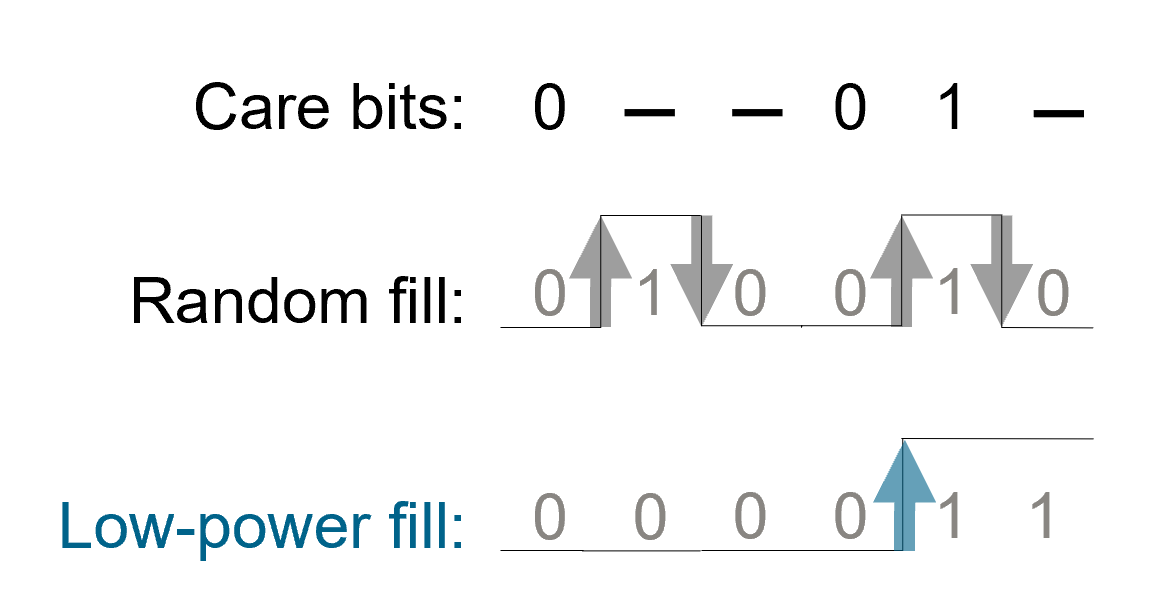
Fig. 7: Replicating care bits for low power shift.

Fig. 8: Shift Clock 1 and Shift Clock 2 staggered during shift phase to reduce shift power.

Fig. 9 Disabling activity of high fanout combinational logic to reduce power.
Another level of reduction in the switching activity during shift can be achieved by selectively turning off the scan chains on a per-pattern basis using the hardware in the test compression logic. In this method, the ATPG tool considers the impact on test metrics and power to determine the disable values which are loaded into shift power control (SPC) chain to control scan chain switching as shown in figure 10.

Fig. 10: Low power shift using SPC chain in compression logic.
For the capture phase of the test, it is crucial to ensure that the peak switching activity due to the at-speed clock pulses stays close to the functional switching activity specification of the device. Clock-gating is one of the most effective techniques used to control power during the functional operation of the design. Since the capture phase of the at-speed test is equivalent to a few clock cycles during the functional operation, the same clock-gaters can also be used to reduce power during test. The power-aware ATPG tool can extract the clock-gating structure during design analysis and configure the logic to selectively disable the clock-gaters to meet power and test requirements.
In conclusion, as power continues to be an increasingly important factor in the chip design process, low-power design techniques are used to meet the power constraints during the functional operation of the chip. This requires test solutions to preserve the functional power intent of the design during the DFT implementation and generate test patterns that stay within the chip power budget during testing. For the next generation of chip designs, it is crucial that designers adopt power-aware test solutions that support power-aware DFT implementation in order to meet the SoC power requirements and provide power-aware ATPG capabilities in order to optimize the test power, cost and quality.
 |
 |
 |
 |
 |
 |
 |
Leave a Reply