Tiny graphene pores; disappearing carbon circuits; performance cloning.

Tiny graphene pores for sensors
In fundamental work that will likely guide current and future graphene membrane design principles in years to come, MIT researchers have created tiny pores in single sheets of graphene that have an array of preferences and characteristics similar to those of ion channels in living cells, and which could be useful as sensors.
The researchers pointed out that each graphene pore is less than 2nm wide, making them among the smallest pores through which scientists have ever studied ion flow. Each is also uniquely selective, preferring to transport certain ions over others through the graphene layer.
They noted that there is a lot of diversity in the transport properties of these pores, which means there is a lot of potential to tailor these pores to different applications or selectivities.

Researchers created pores in a graphene sheet (in purple) and then placed it over a layer of silicon nitride (in blue) that had been punctured by an ion beam. This allows specific hydrated ions, which are surrounded by a shell of water molecules, to pass through. (Source: MIT)
As sensors, the graphene nanopores could be used to detect ions of mercury, potassium, or fluoride in solution. In the future, it may be possible to make graphene nanopores capable of sifting out trace amounts of gold ions from other metal ions, like silver and aluminum.
Disappearing carbon circuits
Using carbon atoms deposited on graphene with a focused electron beam process, Georgia Institute of Technology professor Andrei Fedorov and collaborators have demonstrated a technique for creating dynamic patterns on graphene surfaces that could be used to make reconfigurable electronic circuits, which evolve over a period of hours before ultimately disappearing into a new electronic state of the graphene.
Graphene is also made up of carbon atoms, but in a highly-ordered form, they said. Beyond allowing fabrication of disappearing circuits, the technology could be used as a form of timed release in which the dissipation of the carbon patterns could control other processes, such as the release of biomolecules.
“We will now be able to draw electronic circuits that evolve over time. You could design a circuit that operates one way now, but after waiting a day for the carbon to diffuse over the graphene surface, you would no longer have an electronic device. Today the device would do one thing; tomorrow it would do something entirely different,” Fedorov explained.
The project began as a way to clean up hydrocarbons contaminating the surface of the graphene but the researchers soon realized they could use it to create patterns, utilizing the amorphous carbon produced via electron beam “writing” as a dopant to create negatively-charged sections of graphene. They were initially perplexed to discover that their newly-formed patterns disappeared over time. They used electronic measurements and atomic force microscopy to confirm that the carbon patterns had moved on the graphene surface to ultimately form a uniform coverage over an entire graphene surface. The change usually occurs over tens of hours, and ultimately converts positively-charged (p-doped) surface regions to surfaces with a uniformly negative charge (n-doped) while forming an intermediate p-n junction domain in the course of this evolution.
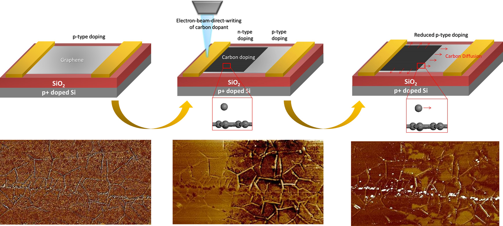
A next-generation additive nanolithography tool enables direct writing of carbon dopants on graphene for reconfigurable functional device applications. This highly controllable, facile doping strategy is expected to advance low-dimensional nanomaterial electronics. (Credit: Fedorov Laboratory, Georgia Tech)
“The electronic structures continuously change over time,” Fedorov explained. “That gives you a reconfigurable device, especially since our carbon deposition is done not using bulk films, but rather an electron beam that is used to draw where you want a negatively-doped domain to exist.”
Beyond the potential security applications for disappearing circuits, the researchers see the possibility of simplified control mechanisms that would use the diffusing patterns to turn processes off at preset intervals. The technique might also be used to time the release of pharmaceuticals or other biomedical processes.
Performance cloning
To help computer chip designers improve memory systems, North Carolina State University researchers have developed software using two new techniques that rely on “performance cloning,” which can assess the behavior of software without compromising privileged data or proprietary computer code.
Given that chip makers try to design their chips to provide the best possible performance, to find the most effective designs, manufacturers need to know what sort of software their clients will be using.
“For example,” explained Yan Solihin, an associate professor of electrical and computer engineering at NC State and an author of two papers describing the new techniques, “programs that model protein folding use a lot of computing power, but very little data – so manufacturers know to design chips with lots of CPUs, but significantly less memory storage than would be found on other chips.
At the same time, many large customers – from major corporations to Wall Street firms – don’t want to share their code with outsiders, which makes it tough for chip manufacturers to develop the best possible designs.
The researchers suggested one way to address this problem is through performance cloning. The concept behind this is that a chip manufacturer would give profiler software to a client. The client would then use the profiler to assess its proprietary software, and the profiler would then generate a statistical report on the proprietary software’s performance. That report could be given to the chip manufacturer without compromising the client’s data or code.
The profiler report would then be fed into generator software, which can develop a synthetic program that mimics the performance characteristics of the client’s software. This synthetic program would then serve as the basis for designing chips that will better meet the client’s needs, the researchers said.
Researchers have now developed software using two new techniques to help optimize memory systems. The first technique is called MEMST (Memory EMulation using Stochastic Traces), which assesses memory in a synthetic program by focusing on the amount of memory a program uses, the location of the data being retrieved and the pattern of retrieval.
The second technique, called MeToo, focuses on memory timing behavior – how often the program retrieves data and whether the program has periods in which it makes many memory requests in a short time. Memory timing behavior can have a significant impact on how a system’s memory system is designed.

 |
|
 |
 |
 |
 |
 |
 |
Leave a Reply