Diverse identifier technologies enable fingerprinting for all device types.

Semiconductor components increasingly require unclonable and tamper resistant identifiers, which are especially necessary as devices become increasingly heterogeneous collections of chiplets and subsystems. These fingerprints provide traceability, which contributes to process improvements and yield learning and enable tracking for a tightly managed supply chain.
While some of this technology has been available for years, continuous development now enables unique identifiers for any electronics component — and just in time, because much has changed. An increasing number of electronic components are being used in cars, medical devices, industrial applications, and data centers, where the impact of substandard counterfeit could be devastating. In addition, system designs are including more secure computing applications that depend upon unhackable private keys. So multiple objectives are driving the interest in unique identifiers that can be read throughout a device’s lifecycle.
It’s important to note that not all identifier technologies are compatible with all fab and assembly processes. But increasingly, the industry recognizes the need to track production parts from cradle to grave, including how chips are disposed of. The applications include connecting data across manufacturing steps, providing keys for security purposes, and identification of counterfeit and used chips.
Within semiconductor design and manufacturing, unique identifiers (a.k.a. fingerprint) can be attached to a design, wafer, die, packaged part, or board. Optically readable IDs for wafers, assembly substrates, and packages are readily supported. For digital ICs, individual dies typically contain electronic chip IDs (ECIDs) with a written wafer ID and x,y location into a one-time programable (OTP) circuit. These identifiers support unit-level traceability (ULT), which links a component to its path through manufacturing process. Such data is valuable for process and yield learning.
“We have an incredibly complex landscape of data. If you track one wafer, it can be split off from the main lot for pre-processing, post-processing, or rework,” said Dieter Rathei, CEO of DR Yield. “Even in these cases, you may want to do a tool correlation. Unique wafer IDs make this possible, while taking into consideration these special cases that can happen on the manufacturing floor. You have to provide solutions that the engineers and fab operators can work with, and also make it as simple and as user friendly as possible within this complex data landscape.”
A unique identifier for a physical electronic device also can support security applications for trusted systems, but effectiveness can vary by identifier technology. For example, while writing fused-based key storage is convenient, it can be compromised. As a result, design engineers often choose physically unclonable functions (PUFs) instead. These circuits rely upon inherent manufacturing variation to create a device specific, and tamper resistant identifier.
“A good analogy for SRAM PUFs are human biometrics, e.g., fingerprints, which are used to identify people,” explained Geert-Jan Schrijen, CTO and co-founder at Intrinsic ID. “SRAM PUFs establish an unclonable anchor, which is collision-free, in the hardware of chips. On top of this anchor different identification/authentication systems can be built, similar to how human biometrics are used in passports.”

Fig. 1: Fingerprints and unclonable identities. Source: Intrinsic ID
As the number of ICs designed with PUFs grows, so do the applications beyond security and traceability.
“Physical identifiers linked to assets from chip design and manufacturing provide a foundation for establishing a trusted digital thread for component traceability and related metrology and test data,” said Tom Katsioulas, IoT advisory board member for the U.S. Dept. of Commerce. “This can be enriched with more identifiers downstream for a hardware bill of materials (HBOM), software BOM, and digital BOM of chips, systems, software apps, and digital twins. The collective trusted digital thread of metadata and information across value chains will give rise to XaaS [anything as a service] business models, and digital marketplaces that will strengthen supply chain resilience and fuel digital economies worldwide.”
Identifier technology options
To be useful, an identifier needs to be unique and readable in an automated factory environment, and in some cases it needs to be extended beyond the factory. But this also can create a management challenge with various multi-step manufacturing processes, where it is not uncommon to have multiple identifiers on the same device. Secure use cases also require the identifier technology to be unclonable and tamper-resistant, and to provide an attestation method.
To choose a device identifier, engineering teams need to consider their functional needs and their process constraints. For instance, digital designs can utilize on-die PUF circuitry, while analog/mixed-signal design cannot. In addition, reading PUFs requires powering up a device, which is not possible in all usage scenarios.
Optical IDs and ECIDs
During wafer and assembly production, engineers have long used optical IDs and OIPs. Wafer IDs are laser-scribed on to a wafer, typically in 18 characters. Die IDs also can be laser-scribed, but often digital designs use ECID technology.
“An ECID provides a unique identifier to each chip or die within a wafer,” said Melvin Lee Wei Heng, senior manager of applications engineering for Onto Innovation. “An ECID contains the x,y location in the wafer, lot information, wafer number, and test program used. ECIDs are normally written into a portion of the chip (during the functional sort programs after a fab process, but before dicing) and can be read out with the right program code via a test program through the I/O pins of the chip.”
ULT is a standard assembly process. During the assembly process factories use optically read IDs on substrates and package lids.
“In the first step of surface mount devices, each substrate comes with a 2D ID (14 x 14 or 16 x 16 dot matrix). It encodes the lot number, substrate position on the panel. The 2D ID now becomes a tracking ID for each individual package. Substrates travel in a flat boat with pockets — a substrate per pocket,” said Gerard John, senior director of chiplets/FCBGA business unit at Amkor Technology. “As the substrate moves through the assembly process at each stage, a camera scans the substrate ID. The 2D ID and associated process and equipment are recorded.”
During encapsulation, the final packaging step, a unique 2D barcode [1] is scribed on the package. It’s then tied to the substrate ID, thereby connecting it to the device’s manufacturing history.
As a device/substrate moves through a manufacturing line its location is known. This is considered a ‘virtual identifier,’ because this specific information, i.e., substrate type + substrate ID + layout specifier + x + y uniquely identifies a physical asset during manufacturing.
“I make a distinction between physical and virtual identifiers,” said Dave Huntley, business development director at PDF Solutions. “To guarantee traceability, you should have a virtual identifier thread, which allows you to trace everything — analog devices, and even passives, during the manufacturing process. On top of this, you want to add these physical identifiers. They anchor a device into the real world, because there is something you can read or measure.”
On-die PUF
Designer teams have been migrating to on-die PUFs to create a unique identifier, in large part because as advanced CMOS shrinks, non-volatile memories used for ECIDs are becoming unreliable. Creating a root of trust (ROT) requires an entropy source for the base key. On-die PUFs rely on inherent process variation during the semiconductor manufacturing process, thereby making it impossible to predict, clone, or modify a chip ID.
SRAM is a particularly useful platform for PUFs because their power-up state provides an excellent source of entropy. [2] “An SRAM PUF is based on the behavior of standard SRAM memory that is available in any digital chip,” said Intrinsic’s Schrijen. “Every SRAM cell has its own preferred power-up state, resulting from random differences in transistor threshold voltages that depend on uncontrollable deep sub-micron variations in local silicon properties. Hence, an SRAM memory yields a unique pattern of zeroes and ones in its power-up state. This pattern is like a chip’s fingerprint, since it is unique to a specific SRAM and hence to a specific chip.”

Fig. 2: SRAM PUF technology. Source Intrinsic ID
SRAM PUFs use only a portion of an embedded SRAM, with 256 or 1,024 bytes being the most common. A small portion of very-well balanced SRAM bit cells result in changes in their power-up state, which results in an inconsistent fingerprint. The full solution requires filtering out these noisy bits.
“A key extractor takes as input the noisy fingerprint and extracts a stable value output,” Schrijen explained. “For chip fingerprints we adopted this approach, which is used for human fingerprints and other biometrics. It requires a good implementation. That’s why we have invested in better algorithms. The extractor uses error correction to get rid of the noisy bits. Next, it uses compression to make sure that you get a full entropy output.”
These algorithms can be implemented in hardware or in software. “The great advantage of an SRAM PUF is that it is present from the birth of the chip, it is inherent in every chip. Intrinsic ID has hardware IP solutions that need to be built-in at chip design time. But with SRAM PUFs, a device-unique identifier can also be retrofitted on any existing device that has SRAM available,” Schrijen said.
As CMOS processes evolve and shrink, design engineers improve upon SRAM PUF technology and explore different manufacturing entropy options. In a recent paper, Intel engineers described a NFET PUF using hot-carrier injection stress to lower the bit error rate to near zero. [3] ICTK Holdings offers a novel PUF structure based upon via resistance, in which deliberate violation of design rules provides the source of entropy. [4]
Another source of entropy is oxide quality differences. [5] “NeoPUF, a quantum-tunneling PUF, is formed by applying identical high electrical fields to a pair of adjacent MOSFETs that have variations in their oxide quality. By using every two adjacent MOSFETs to repeat the process as above, a block of unpredictable and random numbers will be created because it is impossible to know which of two adjacent MOSFETs has a better oxide quality,” said Meng-Yi Wu, research and development director at PUFsecurity. “Once this formation is done, it will not be affected by variations in the environment such as noise, temperature and voltage variations. The stored data “1” and “0” depend on the tunneling current. Because there are no charges stored on the device, after the power is turned off, the PUF derived from this technique cannot be physically traced.”
The physics at work involve oxygen dangling bonds in a gate oxide, which impacts the tunneling current from the silicon substrate to the metal gate. “If there are many dangling bonds (either silicon or oxygen dangling bonds), due to quantum tunneling, an electron has a high probability of hopping from one dangling bond to another dangling bond, which contributes to electrical current,” wrote Charles Hsu, chairman and president of PUFsecurity. “Whereas in a structure with no dangling bond, an electron has a very small chance of jumping from a silicon substrate to a metal gate.” [6] Comparing the electron energy band diagrams of the metal gate oxides further illustrates the basis of these PUFs. In a device with more oxide traps an electron requires less energy to cross the energy band.
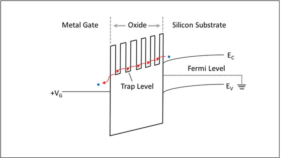
Fig. 3: Electron energy band diagram of MOS (metal-oxide semiconductor) to illustrate electron tunneling through a gate oxide if there are many dangling bonds (oxide traps) in the oxide. Source: PUFsecurity
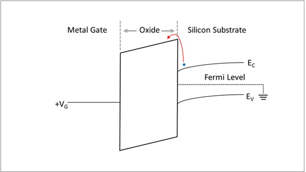
Fig. 4: Electron energy band diagram of MOS (metal-oxide semiconductor) to illustrate the difficulty for electrons to tunnel through the oxide if there are no traps in the oxide. Source: PUFsecurity
Another option is to leverage on-die parameter monitors to create a unique chip ID.
“The proteanTecs Supply Chain Security (SCS) solution is based on generating a signature based on measured in-chip parameters and their dispersion and variability,” said Nir Sever, senior director of business development at proteanTecs. “The advantage of such a signature is that when analyzed using advanced analytics, not only can we suggest if this device is authentic or not, but also, what makes it suspicious and provides root cause guidance. On-die agents (monitoring IP) collect a large set of parametric measurements from each chip, which are then uploaded and fused using machine learning (ML) algorithms to provide alerts and insights. proteanTecs’ XPUF is a pure hardware solution that generates a unique ID generator. It creates a random, unique hardware key per chip as early as wafer sort based on process parameter variations, thereby creating a hardware-based unique ID that cannot be modified or hacked, establishing a solid root of trust.”
Externally applied PUF
The defense, safety-critical, and automotive sectors demand secure unique identifiers for digital ICs, passives, analog/mixed-signal ICs, and all the way to a final module. But not all IC processes can support ECIDs or on-die PUF solutions. Fortunately, engineers can avail themselves of externally applied technologies. These technologies either add material or inscribe data in the device material.
“The FemtoTag tool produces an array of nanodots, which contain user-defined information,” said Steve Walters, chief engineer at Aerocyonics. “It utilizes femto-second laser sources, optics, imaging, specialized gas/plasma processing, and machine vision to rapidly add or remove material at a focus point within the sample or on the sample surface. The tool is capable of very rapid removal (1mm3/min) or material deposition onto almost any material with 2nm to 200nm dimensions. The laser transforms the target material to create nano-scale voids, which are uniquely structured so that data is contained in three dimensions, resulting in a high-density (10kbits/mm) marking with unique structural attributes that make it unclonable. Additionally, data content can be either encrypted, unencrypted, or a combination of both. Data content is user-defined and is not restricted in quantity, given the tag size is variable based on content. The tag is passively read using one of several modalities. If visual line of sight is available, the tag can be read optically. Without line of sight, the tag can be read using X-ray or the FemtoTrace terahertz reader. This allows reading of tags buried within a device — for example, a die tag within a packaged device.”

Fig. 5: Supply chain traceability with FemtoTag. Source: Aerocyonics
Another identifier uses diamond particle tags, or “DUST”, to form a unique identifier.
“DUST stands for diamond unclonable security tag,” said Ophir Gaathon, CEO of DUST Identity. “We use the waste material that comes from the abrasives industry. These diamonds are too small to be used as abrasives. We put them into the form factor of very small dust particles — micron to sub-micron. By having those particles land on the surface of an object, or being inside a coating, a multi-dimensional pattern can be formed. The particles are suspended inside a transparent plastic or urethane. The configuration of the suspended particles creates a very hard to replicate ID. We validate it using optical methods.”
This technology can be applied to every component in the electronics supply chain. “DUST is a component-agnostic (digital, RF, AMS, passive, board, etc.) physical identifier, which can be applied in the field with an applicator or at a final process gate,” Gaathon said. “Going from right to left in the supply chain, a distributor may spray DUST on an existing reel of components. An OEM can adapt its commercial line and apply DUST for secure traceability requirements of NDAA Sect 5949 for use in critical systems. An OEM can integrate DUST at a feasible cost across its entire population at module final test through integration with the epoxy molding compound (aka plastic).”
Manufacturing use cases
Identifiers lie at the center of traceability in a semiconductor’s manufacturing life. Naturally, engineers use them for feedback for yield and quality improvement, especially between suppliers. For instance, substrates located at a specific corner of a panel exhibit a higher failing rate at final test. This information gives a clue about the root cause. Or, the cause could be assembly or substrate-process related.
The ability to pre-fetch data from a previous test step affords smarter decisions regarding pass/fail. “The immediate usage case is data feed forward– pulling forward from previous insertion and taking advantage of at a later insertion,” said Ken Butler, senior director of business development at Advantest America. “For example, the data can support outlier analysis or test content reorder. Consider final test. Once you power up the chip and read the ECID, you can link back to wafer lot and wafer ID and pull the data. Or maybe you’ve already pre-fetched a wafer lot’s data, but your final test logic only has five wafers. The ECIDs let you figure out which wafers are in your test lot to limit the data for your inferencing.”
Others agree on the use case for testing real-time analytics that device identifiers enable. “Chip unique identifiers are important and more important when applying data feed-forward and feed-backward applications,” said Eli Roth, smart manufacturing product manager at Teradyne. “You need to identify your part and have its data available in real time, because you can’t afford to go out to a cloud to retrieve the data. You need to have it readily available.”
Conclusion
System designers/owners want a secure and unique identifier that can be accessed from creation to grave, and manufacturers value the benefits of attaching a device’s manufacturing genealogy to an accessible identifier. What’s changed is that engineers now can consider a selection of technologies, and often a device will have more than one identifier.
The applications that a device identifier enables continue to grow, because it can connect a device’s data across the manufacturing processes, it can furnish evidence of a device’s provenance, and it can supply the unclonable identifier that anchors a device to a root of trust. And soon, in order to meet government regulations, sustainability data will be connected to a device. [6] Collectively these will support a trusted digital thread, which will offer new service-based businesses and digital marketplaces.
References
1. https://en.wikipedia.org/wiki/Barcode#Matrix_(2D)_barcodes
2. 2. G. -J. Schrijen and V. van der Leest, “Comparative analysis of SRAM memories used as PUF primitives,” 2012 Design, Automation & Test in Europe Conference & Exhibition, https://ieeexplore.ieee.org/document/6176696
3. R. J. Parker et al., “A Physical Unclonable Function Leveraging Hot Carrier Injection Aging,” 2023 IEEE International Reliability Physics Symposium, https://ieeexplore.ieee.org/document/10118128
4. D. Jeon, J. H. Baek, D. K. Kim and B. -D. Choi, “Towards Zero Bit-Error-Rate Physical Unclonable Function: Mismatch-Based vs. Physical-Based Approaches in Standard CMOS Technology,” 2015 Euromicro Conference on Digital System Design, https://ieeexplore.ieee.org/document/7302303
5. Wu, M. Y., et.al., “A PUF scheme using competing oxide rupture with bit-error rate approaching zero,” 2018 IEEE International Solid-State Circuits Conference, https://ieeexplore.ieee.org/document/8310218
6. https://www.pufsecurity.com/document/puf-series-3-the-quantum-tunneling-mechanism-of-neopuf/
7. https://psqr.eu/publications-resources/all-about-dpp/
Related Stories
Making Sense Of PUFs
What’s driving the resurgence of physically unclonable functions, and why this technology is so confusing.
Making PUFs Even More Secure
New sources of entropy could significantly improve robustness of physically unclonable functions.
Hiding Security Keys Using ReRAM PUFs
How two different technologies are being combined to create a unique and inexpensive security solution.
 |
 |
 |
 |
 |
 |
 |
Leave a Reply