Different types of memory will be necessary for ultra low power and low cost.

There are two things in life that have always been true: One is that you can never be too rich, and second—at least since the dawn of the technological age—you can never have too much memory. But the memory truism is changing with the onset of the .
The next generation of memory for the IoT must meet a different set of metrics – smaller, smarter, lower power, and longer life.
“From an end-device perspective, the big challenges for IoT devices are power consumption, footprint and security,” observes Amit Gattani, senior director of embedded solutions for Micron. Memory is in the wheelhouse for all three of them, although it isn’t a big factor in power consumption, relative to the MCU or the radio,for example.
By 2020, there will be an estimated 25 billion to 50 billion objects on the IoT. No one knows precise numbers, but all the estimates are very large. And the amount of memory these devices will require is astronomical. Still, many of the chips that will manage these devices will be simple and inexpensive and have little room for memory. Other devices, such as those used in the various infrastructures, vehicles, medicine and automation, have a bit more breathing room, although they face a larger issue in the security realm and the sheer volume of data processed.
Power first
Much of what will be found in the IoT will demand ultra-low-power components – from sensors to wearables to medical devices, to motes and Internet dust. Moreover, most of these next-generation devices will be both mobile, as well as low-power, and they will be subject to a myriad of environmental conditions that previous generations of memory did not have to worry about.
In addition, metrics such as size, packaging, integration, interface, performance, temperature, low-power, low-voltage and cell density, all are design criterion that vary widely from segment to segment. Add to that new or emerging technologies such as energy harvesting, and this puts a new spin on IoT memory.
But we still have a long way to go on many of these parameters, particularly in areas such as energy harvesting.
“We are not yet at the point yet where energy harvesting (EH) technologies that utilize such sources as ambient RF energy or micro-motion are workable for the IoT,” says Steven Woo, vice president of enterprise solutions technology at Rambus. “However, what people are hoping is that mechanisms for EH will become more efficient, while at the same time chip power utilization will drop, and we get to a point where the integration of these become more realistic. That is, kind of, where the chip community is heading.”
At least part of the solution also is on the architecture side, which is getting far more attention these days. “One of the things learned, when you study chip architecture, is that anytime you go off-chip, to do anything, it is very expensive from a power standpoint,” Woo said. “So the first consideration, is never go off-chip, if possible.”
That works its way into memory as well. Memory devices will play as key a role in the IoT, as they have in classic computing devices and almost all other electronic devices today. They will continue to house the functional system code, working parameters, data, and any other system functions. The gotcha is that they now must be smaller, lighter, and denser. And simultaneously they must be fast, reliable, ultra-low power, and secure.
“Endpoint security is important” notes Gattani. “You don’t want your endpoints to be spoofed so endpoint identity has to be solid and have the right code. That means memory security is tantamount and there are some things coming down the channel that will help to address that.”
Consider sensors and early IoT wearables, for example. In many cases they are relatively simple circuits that accept input, deal with it according to the requirement, and either forward, or store for later retrieval. Such devices generally do not require high density memory or extensive computing power. Therefore, their power requirements usually can be met with most low-power solutions.
On the other end of the spectrum, shrinking the equivalent of a smart phone or tablet’s functionality down to an IoT device will require a fair amount of tinkering. This is because such devices will require a lot of memory and computing power, which is a real challenge for low-power platforms.
(The low-power MCU angle will be addressed in an upcoming article. This article will focus on what is emerging in next-generation memory.)
OTP — the memory solution?
Volatile memory isn’t going to cut it for most of the objects on the IoT. There isn’t enough bandwidth, in terms of footprint, power and economies of scale for the inexpensive and simpler devices that will make up the majority of the IoT objects. On the higher end of the scale, in industries such as medical, infrastructure, defense and aerospace, there is a bit more wiggle room. But even those industries will certainly see utilization of non-volatile memories (NVM). Power is now a critical design criteria everywhere.
Most popular non-volatile memory (NVM) technologies are either flash or EEPROM (see note 1). DRAM is the standard volatile technology. The combination of these have been the de facto memory platform for pre-IoT devices and systems to date. Power requirements for such devices are high, and the present state of such technology is not a good fit for a large segment of IoT devices. However, emerging and evolving derivatives of these technologies are appearing that will meet the requirements of the IoT.
One of the more promising technologies is the efuse, antifuse, and floating gate one-time programmable (OTP) type memory. The nice thing about the current crop of such memory is that it can be implemented on standard, mature CMOS technologies, leveraging the economic advantages of both CMOS and established processes.
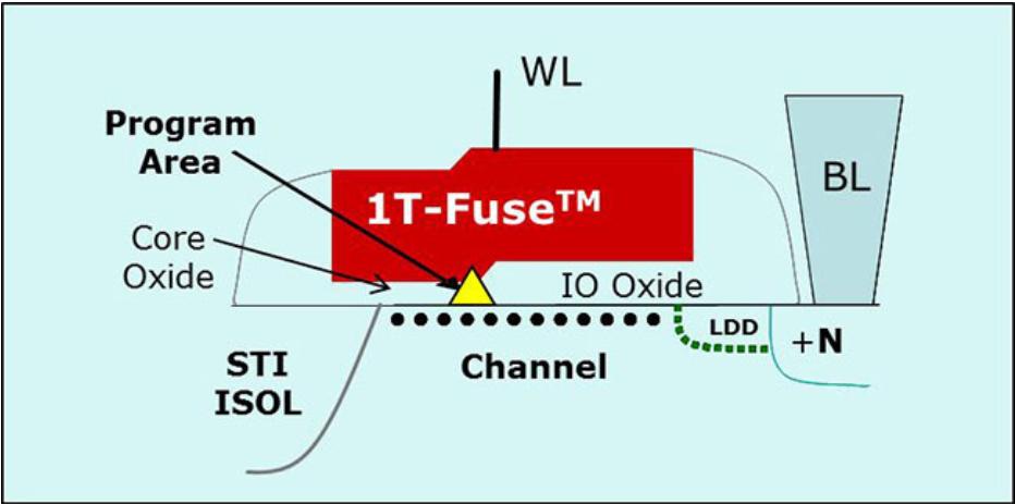
Figure 1. Typical fused cell. Courtesy Sidense Corp.
OTP memory, as the acronym implies, is a type of memory that can be programmed only once. It is a “fused” cell that either has the fuse intact, or is blown, representing a logical 1 or 0. The 1 or the 0 is based on the state of the OTP memory elements (shorted or open). Which state corresponds to the logic 1 or 0 is generally application specific (see Figure1).
A typical floating-gate device uses what is called a stacked-gate 1T cell. This is a MOS transistor with one floating gate and one contacted gate that overlap each other (see Figure 2). This technology is also available in MTP, and there are other variants as well.
There are multple benefits to using OTP memory. First , it is inexpensive and tiny – one transistor, typically, as compared to floating-gate multi-time-programmable (MTP) memories. Second, it requires no power to hold the state. Physical arrays are compact, which lowers capacitance of the bit and word lines, thereby reducing pre-charge and switching power consumption. And, it can be implemented on standard CMOS technologies.

Figure 2. Typical fused cell. Courtesy Kilopass Technology.
The downside of this is the same as the upside. It only can be programmed once. However, for a wide range of IoT devices, that may be all that is required. And, if there is limited reprogramming required, extra OTP blocks can be placed into the circuit that can be programmed in the future to update or modify the device functionality or contents. This allows such memory to emulate multi-time programmable (MTP) devices. Typically, this is used for code patching, updating or functionality improvements/additions where small elements of code can be updated, in contrast to having to update the complete code footprint.
A huge advantage, innate to OTP memory, is security. OTP memory can implement anti-piracy solutions on ICs. It is a simple and effective low-cost approach that uses a random number generator to create a unique identification number, which is permanently coded into part of the memory. The number is virtually impossible for pirates to detect, especially if a large integer RNG is used, because there can be billions of possible combinations. And there is no way to change the ID number in NVM. Moreover, OTP eliminates the security issues that are associated with field-programmable masked ROM.
Related platforms
There are several variations of NVM technologies that can act like multi-time programmable (MTM) memory. MTP technologies include EEPROM, Flash, RRAM/MRAM (magneto-resistive/resistive random-access memory), FRAM (ferroelectric random-access memory – also known as FeRAM and F-RAM), SONOS (silicon-oxide-nitride-oxide-silicon), and phase change memory (PCM).
RRAM uses a rather novel technique to store data. It uses resistance to store each bit of information, so only very small increments of power are required. This makes it a perfect solution to some of those very tiny IoT devices such as motes and Internet dust. RRAM changes state by changing resistance, by applying a small voltage. The change sticks until the next write.
FRAM, meanwhile, boasts low-power and fast writes. It has a structure similar to DRAM, but the data is stored by polarizing a ferroelectric material (Lead-Zirkonate-Titanate). As an electric field is applied, dipoles shift in a crystalline structure to store information. On the security end, code and data stored in FRAM are less vulnerable to attackers than Flash/EEPROM, and are resistant to radiation EMI/RFI.
SONOS memory uses an insulating layer, such as silicon nitride, to hold state. This type of NVM is also known as charge trap memory because traps in the nitride capture the charge carriers and retain the charge that is injected from the channel of a MOS device. This makes such memory less sensitive to what is called pinhole defects, and tends to be robust in terms of yield and data retention.
PCM is one of the technologies proposed as a replacement for NVM NAND. PCM changes states by rapidly heating chalcogenide glass. When heated, the glass shifts between its crystalline and amorphous state. In its amorphous state the structure has very high resistance (which is read as a binary 0). In the crystalline state, resistance is quite low (which is read as a binary 1). Such memory can quickly shift between the two states, making it an attractive option in the NVM pool. Recent research in this technology has shown that it may be capable of intermediate states as well. Such states allow two bits, instead of the usual one, to be stored in each cell.
These advanced NVM technologies show a lot of promise for a number of reasons. They promise better overall performance figures than typical NVM technologies such as NAND and NOR flash, and E/EEPROMS. They offer faster write speeds, lower voltage and power requirements, better data retention, are longer lasting, have better resistance to environmental influences are scalable and many can be implemented in mature CMOS. A quick list of benefits is listed at the end of this article.
Conclusion
There is general agreement that the IoT will have untold numbers of interconnected data-gathering and data-processing devices. These billions of computing systems, controllers, sensors, and communication systems, unfolding in an evolving IoT ecosystem. Will present a myriad of challenges in embedding memory and MCUs. The gamut of simple to highly complex devices will present numerous opportunities for various types of embedded memories.
Sometimes, what is old is new again, for years, the DRAM envelope has been pushed to achieve faster, better performance. But tomorrow, the IoT is pushing the pendulum in the opposite direction – back to the technology that started it all. Indeed, what is old, is new again.
Note 1 Flash memory is a form of electrically erasable programmable read-only memory (EEPROM). The difference is that E, and EEPROMs, had to be completely erased before being rewritten, Flash memory may be written and read in blocks (or pages) rather than having to erase the entire device. Benefits include low manufacturing costs and easy and simple integration into logic baseline process. Because there are no changes to baseline Si models, existing design IPs are preserved, allowing IP re-use and faster time to market. It also is compatible with existing semiconductor dies, easy to test with a high intrinsic yield, and it allows flash and EEPROM, as well as NVM, to be used on the same chip.
 |
 |
 |
|
 |
|
 |
Well explained! I wonder what the next solution is for DRAM after 20nm for some of the leading companies (Micron, SK Hynix, and Samsung)? Can we expect a next planar shrink or is it more feasible to see new technology. Which planar shrink is feasible and which of these new technologies are front runners?