Stochastics effects are the ultimate limiter of optical lithography technology and are a major concern for next-generation technology nodes in EUV lithography.

By Alessandro Vaglio Preta, Trey Gravesa, David Blankenshipa, Kunlun Baib, Stewart Robertsona, Peter De Bisschopc, John J. Biaforea
a) KLA-Tencor Corporation, Austin, TX 78759, U.S.A.
b) KLA-Tencor Corporation, Milpitas, CA 95035, U.S.A.
c) IMEC, Kapeldreef 75, 3000, BE
ABSTRACT
Stochastics effects are the ultimate limiter of optical lithography technology and are a major concern for next-generation technology nodes in EUV lithography.
Following up on work published last year, we compare the performance of organic chemically-amplified and condensed metal-oxide resists exposed at different sizing doses using a proxy 2D SRAM layout.
For each combination of material, technology node, and lithographic approach, we perform 550,000 physics based Monte-Carlo simulations of the SRAM cell. We look at many performance data, including stochastic process variation bands at fixed, nominal conditions assuming no variation in process parameters vs. the stochastic process variation bands obtained by inclusion of the effects of process variation. These perturbations are applied where we expect natural variation in the process to occur: exposure dose, focus, chief-ray azimuthal angle, mask CD, stack thicknesses, and PEB temperature.
We study stochastic responses for three technology nodes:
For each case, we optimize mask bias, source illumination and process conditions across focus to maximize the optical contrast. We did not apply optical proximity correction to the mask.
The purpose of the work is to evaluate the stochastic behavior of different features as a function of material strategy, technology node, and lithographic approach.
Keywords: EUVL, SRAM, PW, CDU, NILS, PPM, stochastic
1. INTRODUCTION
In previous work1, the authors showed how we modified the PROLITH X6.0™,2 electron-scattering model for EUV resists to capture differences in the electronic response of organic, metalorganic (organic with metal-particles), and metal-oxide platforms. To evaluate the lithographic performance of these materials, we compared figures of merit such as Critical Dimension Uniformity (CDU), pattern Placement Error (PE), and failures per million, simulating one million stochastic contact holes (CHs) for each combination of material and technology node. In agreement with experimental data3,4,5, we found that the CD distributions at best conditions (best dose and focus) deviate from true Gaussian behavior, showing increasing skewness and kurtosis4,6 when absorption, aerial image contrast, or exposure dose are decreased and blur length is increased. Even at 7 nm technology node (N7), a non-negligible asymmetry in the left-right σ of the CD distributions can lead to missing CHs if a large enough population is considered.
The current failure rate specification for some semiconductor applications is in the Parts Per Million, Billion or Trillion (PPM, PPB, PPT), which requires significantly more than 6σ feature control, as reported in Figure 1. The use of 550,000 trials allows a statistically valid 4σ analysis.

Figure 1: Probability plot as function of σ. PPM, PPB, PPT respectively stand for parts per million, billion, trillion.
In this paper, we use the same methodology used in reference 1, substituting a metal layer for an SRAM proxy cell and simulating its performance vs. technology node, resist platform, and lithography approach.
2. MODELING AND DATA ANALYSIS
Imec7 designed the SRAM proxy cell used to simulate N7 (Figure 2 left). For the metal level, the dense pitch in x direction is 42 nm, with a feature width of 21 nm. The target CD for these short lines and the spaces between is 21 nm. The gap CD in the y direction measures 25 nm.
An approximation of a cell for 5 nm technology node (N5) is produced by reducing the dense pitch to 38 nm and the gap CD to 21 nm, using a scaling factor of 0.905 in x and 0.851 in y direction. The cell for 3 nm technology node (N3) is approximated using a horizontal half-pitch and a gap CD of 17 nm with x and y scaling factors of 0.895 and 0.790 respectively, according to analysis published by imec8.
For each node, we optimized illumination and mask biases across 60 nm of focus. Simulations are performed at best focus and best dose except when otherwise specified. We did not apply Optical Proximity Corrections (OPC) to any node.
We used three calibrated resist models to simulate each cell: an organic Chemically Amplified Resist (CAR), a fast-organic CAR, and a metal-oxide resist. All of them have been calibrated using extensive experimental data collected at imec and are reported in previous work1,9,10.
As shown in Figure 2, we measured 26 locations to collect CD, CDU, placement error, number of failures, and absorbed photon density from 10 lines, 8 spaces, and 8 gaps. The averaging length of line and space metrology boxes are equal to the target CD; the gap averaging length is 3 nm. This metrology recipe collects 14.3 million CD data for each combination.

Figure 2: Left: imec SRAM proxy cell metal layer designed for N7 node. Center: N5 cell. Right: N3 cell. The green boxes represent the 26 metrology planes collected for each simulation
a. N7 simulation
For N7, two different sets of simulations were performed using a strong dipole x illumination: ideal case and real case.
The ideal case represents an unrealistic but useful scenario, feasible only by means of computational lithography: all the lithographic parameters are fixed to nominal with no variation; for example, the only parameter varied within the 550,000 simulations is the random seed11,12. The exposure dose was fixed at 45 mJ/cm2, and we chose the best focus using Process Windows (PW) analysis in ProDATATM2.013.
In the real case test, uniformly but randomly distributed perturbations of key parameters were applied to evaluate the effects of defensible variation in the experiment:
b. N5 simulation
For N5, we simulated three different materials with dipole x illumination. The purpose of this experiment is to evaluate how resist platforms influence the pattern failure rate. Exposure doses for the reference organic CAR, the fast-organic CAR, and the metal-oxide material were 35, 17, and 53 mJ/cm2 respectively.
We performed all simulations at best dose and focus (as in the N7 ideal case), changing only the trial number.
c. N3 simulation
We performed N3 simulations with the reference organic CAR at best dose and focus, and selected three different lithographic approaches:

Figure 3: N3 masks and illumination for the three cases. The illumination graph reports the 0th, and ±1st diffraction orders. Graph c) shows a scaled version of the mask by a factor of 2 in both x and y direction.
d. Probabilistic contour analysis
For each of the 550,000 simulated cells, we also extracted contours to locate the weaker spots in the design. The first graph we generated is the edge placement band, similar to what De Bisschop presented in 201415 and reported in 20175. The edge placement band is obtained through Boolean operations considering all the stochastic trials of the cell. Figure 4 shows the evolution of such bands across multiple trials.

Figure 4: Example of edge placement bands vs. number of trials. a) and b): two contours of two different stochastic simulations of the same process. c): overlap of the contours of trial 1 + 2, where the white band is the spatial range of the edge placement. d) and e): edge placement bands when 16 and 550,000 trials are overlapped.
The graphs in Figure 4a, 4b show two stochastic simulations of the same process, where white represents photoresist and green represents the substrate. The red lines represent the edge contours, which are slightly different in each trial (due to stochastic effects). If these two contours are overlapped, Figure 4c is obtained, where the white band represents the spatial range of the edges placement from trials 1 and 2. The last two graphs of the same figure are obtained in the same method, but with additional trials considered (16 and 550,000).
As more randomized contours are added, the more the width of the band increases. In the last graph to the right, the white bands of different lines begin to touch. This does not indicate the probability of a failure, such as a bridge, but it does indicate that the spatial range of opposite contours do overlap, if enough trials are performed.
The second graph used to evaluate the results uses the probability of finding photoresist as a function of position (Figure 5a) over 550,000 different trials. The graph is plotted in Log10 scale, where 0 (yellow) indicates that resist is found with a probability equal to unity across all trials, while -5.74036… (dark blue) indicates that resist is never found (space). The spectrum of colors in between is representative of the stochastic variation evident in the process. It is therefore straightforward by inspection of the plot to locate areas where ‘black swan’ events4,16 – failures with very small probability of occurrence – may arise.

Figure 5: a): Probability of finding resist in Log10 scale generated by 550,000 simulations. On the right, a particular location is enlarged, where the layout is prone to fail with a probability of 1 in 10000. b): aerial image at threshold to target (grey) and mask polygons (blue). c): σ contours extracted from a). The black contour represents the 1σ resist distribution, equivalent to finding the resist edge in that particular location in at least 68% of the cases. Blue, green, and red represent 2, 3, and 4σ, respectively.
From this graph, it is possible to extract contours representing consecutive σ of the edge placement. In Figure 5c, 1, 2, 3 and 4σ are shown respectively in black, blue, green, and red.
It is also interesting to compare the aerial image in Figure 5b with the σ contours in Figure 5c. While the aerial image seems quite aligned with the mask (or design in this case), the σ contours – which are “stochastic aware” – clearly show bridging mechanisms between the ends of neighboring lines, appearing most prominently especially at the 4σ contour.
3. RESULTS
a. N7 simulations: ideal vs. real case
Table 1 shows results for the N7 ideal and real case simulations. See section 2.a for an explanation of the setup.
Table 1: Results for N7 ideal (top) and real (bottom) case. a): edge placement bands. b): resist probability plot. c): normplot graphs of lines and spaces (blue) and gaps (red), and histogram of all the CDs normalized, centered in zero (pink). d) summary tables; NILS stands for Normalize Image Log-Slope.

In both cases, 14.3 million CDs were collected for 550,000 stochastic simulations. The main difference observed is failure rate that, as reported in the table summary at right, increases by an order of magnitude for the real case. Also, from inspection of the normplot4,17 graphs in Table 1c, it is clear that small process perturbations increase the skewness and kurtosis of the gap CD distributions (in red), making black swan events more likely.
b. N7 simulations: ideal case, process windows comparison
Stochastic computational lithography (SCL) can also be used to more accurately evaluate PW. For the ideal case, we reproduced an 18×16 Focus-Exposure Matrix (FEM), simulating each dose-focus combination ~ 2000 times. In Figure 6, we compare the overlapped PW of lines, spaces, and gaps not including and including failures as process window limiters. Both Depth of Focus (DoF) and Exposure Latitude % (EL) are decreased if failures are considered. The printability of these features is therefore not limited by Rayleigh resolution, but by the occurrence of failures18.

Figure 6: Top: PW comparison without (left) and with (right) failures. Bottom: exposure latitude (%) vs. depth of focus comparison.
c. N5 simulations: material comparison
We used the N5 vehicle to compare performance of different materials given the same aerial image quality. Table 2 shows results for organic CAR, fast-organic CAR, and a metal-oxide material. All the simulations are carried out using ideal conditions (best constant focus and dose). The main difference among the three materials is photon absorption: the impact of Photon Shot Noise (PSN) is evident by comparing the organic CAR with its faster version (rows 1 and 2 of the table).
The metal-oxide resist shows normplot distributions that are more Gaussian than those of the CARs, and its the failure rate is at least two orders of magnitude better. These materials generally have the following characteristics:
Table 2: Results for N5 simulated with organic CAR (top), fast-organic CAR (middle), and metal-oxide (bottom) material. a): edge placement bands. b): resist probability plot. c): normplot graphs of lines and spaces (blue) and gaps (red), and histogram of all the CDs normalized, centered in zero (pink). d) summary tables.

d. N3 simulations: across lithographic approaches
Table 3: Results for N3 simulation in single exposures, double exposures, and single exposure with next generation tools, from the top to the bottom row. a): edge placement bands. b): resist probability plot. c): normplot graphs of lines and spaces (blue) and gaps (red), and histogram of all the CDs normalized, centered in zero (pink). d) summary tables.
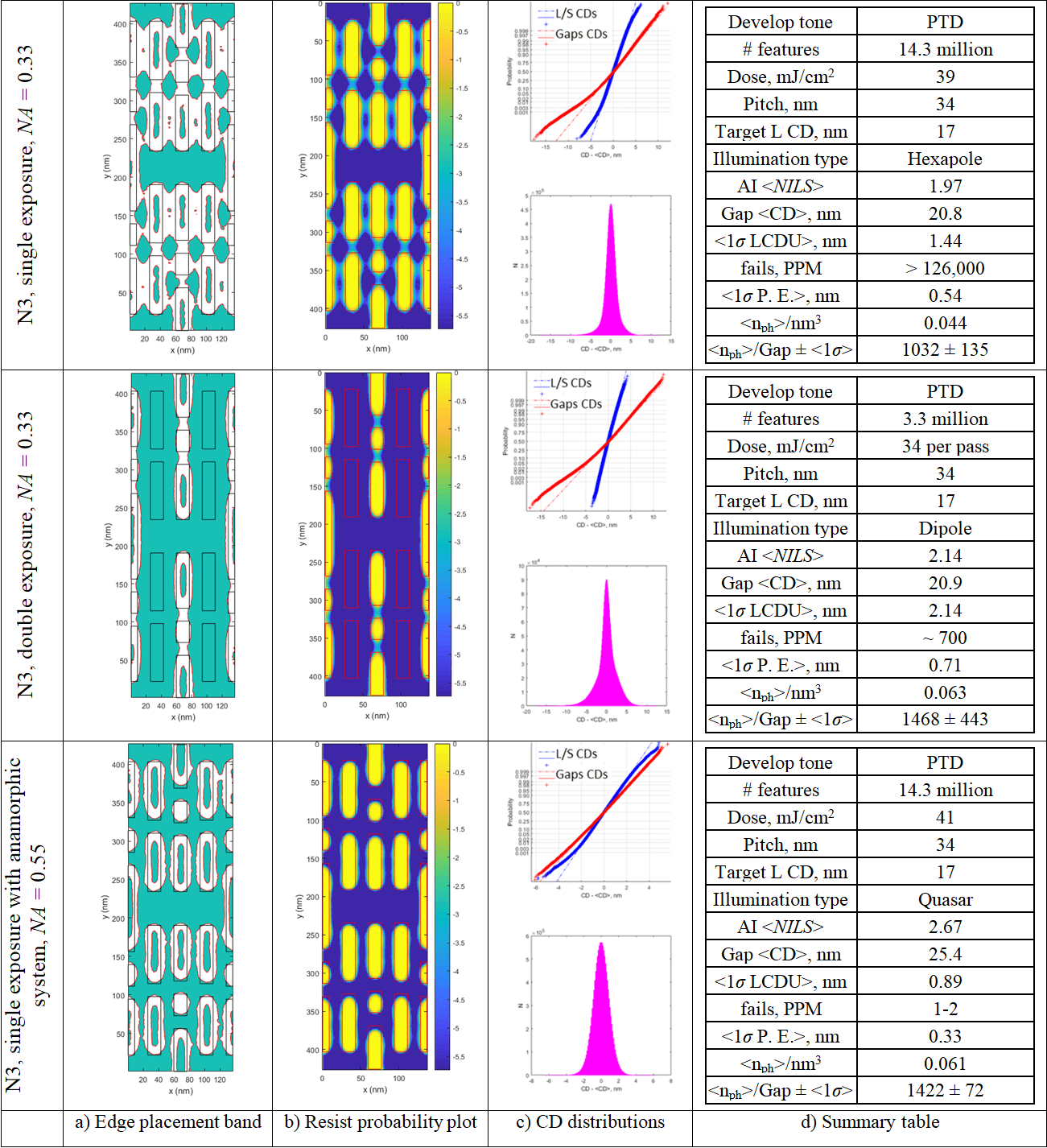
We carried out N3 simulations using ideal case with the organic CAR material only. For this node, we compared three different approaches: single exposure with current EUV tools NA, double exposure (LE2) with current EUV tools NA, and single exposure with anamorphic hyper-NA tool13 (Table 3).
We used the double exposure approach considered in this work to understand if it would generally be possible to print nonperiodic gaps smaller than 20 nm with organic materials and reasonable dose in a pseudorandom 2D design. Relaxing the pitch in the horizontal direction, we could better optimize the illumination to increase the image contrast of such gaps. However, the gap fail rate is ~ 700 PPM, which translates directly in a probability to have 1 pinch in a gap every 350 cells.
Increasing the contrast and relaxing some of the shadowing effects with a hyper-NA anamorphic tool should allow a fail rate comparable to the current N7 situation.
4. CONCLUSIONS
In this paper, we used stochastic computational lithography (SCL) simulation to investigate printing failures of an SRAM proxy in the 5σ regime. We use different physical resist models across technology nodes, 7 to 3 nm. We explored alternative lithography techniques such as double-patterning and hyper-NA anamorphic EUV systems to understand resist and illumination limits for pseudorandom 2D layouts across technology nodes.
The following statements summarize the results:
ACKNOWLEDGEMENTS
The authors would like to thank Heather Spears (KLA-Tencor) for useful discussion. We would like to thank Peter de Schepper, Jason Stowers, Mike Kocsis, Steven Meyers, Michael Greer, Andrew Grenville (Inpria), Satoshi Dei, Kenji Hoshiko, Masafumi Hori and Yusuke Anno (JSR), for the information and the support of photoresists.
REFERENCES
This was originally published in SPIE Advanced Lithography Conference 2018: Proc. SPIE 10583, Extreme Ultraviolet (EUV) Lithography IX, 105830K (19 March 2018); doi: 10.1117/12.2299825
 |
 |
 |
 |
 |
 |
 |
Leave a Reply