Chipmakers wrestle with EOS, ESD and other power-related issues as leading-edge chips are incorporated into industrial and automotive applications.

Stringent safety requirements in the automotive and industrial sectors are forcing chipmakers to re-examine a number of factors that can impact reliability over the lifespan of a device.
Many of these concerns are not new. Electrical overstress (EOS), electrostatic discharge (ESD) and electromigration (EM) are well understood, and have been addressed by EDA tools for years. But as chip complexity and density grows, they are becoming much bigger issues for a couple of reasons. First, some chips developed for these markets are expected to last for 10 to 15 years. And second, the chips themselves are more complicated, so automotive OEMs and Tier 1 suppliers now require more granularity than for other markets.
“Before, the analog blocks were small, the chips were smaller, and you could kind of feel good just running a few handful of SPICE simulations,” noted João Geada, chief technologist at ANSYS. “But when designs have billions of transistors, that’s not a scalable answer anymore.”
Likewise, topology checking tools were effective enough for EOS analysis in the past. “A topology check just sees the gate at a particular transistor and whether a path can be traced to a high-voltage signal, ignoring completely what the state of that path looks like,” Geada said. “It doesn’t really understand voltage regulators and all that kind of trickery that people put on chips these days. For a smaller design, this is a viable strategy. But again, it’s a scale problem. Today, simulation-based approaches are needed to give an answer that matches what silicon does.”
Some of this is market-specific. “When you’re dealing with cell phones or disposable electronics and you get a few failures, so be it,” he said. “But when you’re dealing with industrial electronics, industrial entities or automotive electronics or avionics, these are problem domains. The catch for those is that they have required expected life times. You cannot have an unexplained failure, so all of a sudden reliability becomes a lot more important. It used to be that the reliability space was kind of segregated to much smaller designs, much larger geometry that could be analyzed with more primitive methods. But an ADAS system has hundreds of ECUs and very sophisticated electronics analyzing real-time video streams, and it all needs to be parsed in real time. It’s basically a supercomputer wrapped up inside a car. That scale of electronics cannot be dealt with at our current method of analysis. There must be a more formal, rigorous strategy particularly since the design cycles have shortened.”
For chips used in safety-critical applications such as cars, there’s much more riding on the design being absolutely perfect. “It’s no longer an option to hand wave and say it worked great on the tester. You have to know it continues to work under all possible usage scenarios. Therefore, you need systems that deal with reliability very much like static timing analysis does for timing — a formally correct way of guaranteeing that there is no possible vector in the universe or vectors in the system that can cause an event that causes the chip to fry itself,” he continued.
EOS is central to these concerns. If too much voltage is applied at the gate, it overwhelms the thin dielectric, particularly at advanced nodes, which in turn can destroy the transistor. Under most circumstances, if an EOS event happens, the chip will fail.
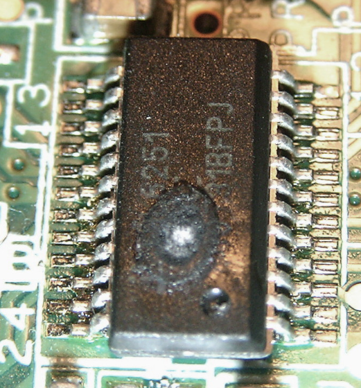
Fig. 1: Result of electrical overstress in laptop IC, where overheating has melted the plastic casing. Source: Wikipedia
EOS generally is caused by a bad design or an unexpected set of patterns that increase the voltage beyond what it can handle. Typically, this happens for a prolonged period of time with a small voltage.
“Most of the cases that we worry about are a volt or thereabouts, but they just persist for a sufficient time to blow the dielectric,” Geada said. “Dielectrics are basically a molecule or two, so they don’t have really the capacity to withstand prolonged electric stresses.”
In contrast, ESD is more typically caused by an outside event. Someone walking on a carpet builds static charge, which is released quickly at high voltage. This is basically the equivalent of lightning striking on a chip, and it requires the same kind of grounding as a lightning rod provides for a building. When an ESD event happens, the device goes outside of its prescribed design tolerances.
“Customers have been asking their foundry, or their internal modeling teams, to model the device and its behavior under these breakdown conditions,” said Matt Hogan, a product marketing manager at Mentor, a Siemens Business. “With a transistor or a diode you’ve got a small signal model, which is the model that a SPICE simulation normally operates under.”
That is used for sub-threshold analysis, which typically relies on a waveform of current voltage characteristics that engineering teams work around.
“When we were learning electronics and transistors, we were told to stay away from this non-linear region down at the bottom, which is the sub-threshold area that everyone is trying to design ultra-low power and asynchronous designs for,” said Hogan. “At the other end of that curve is where ESD events happen. You’re just pushing so much energy through this device and hopefully it’s sized large enough that it’s going to survive. More than likely, your ESD device is the sacrificial device that ends up popping but preserves the rest of your circuit.”
EOS needs to be viewed from a transistor perspective to understand what stresses are being put on the gate oxide, he said. “One of my favorite pictures of that is if you have just a little transistor that’s switched, say 1.8 volts, and you have its bulk connection connected up to say 3.3 volts, you will get an oxide breakdown of that device because the oxide is being pulled up to a voltage that is higher than you were actually switching to. It’s not an immediate failure. It’s a failure over time, so it falls in to this subtle reliability category of simulating it with a SPICE simulator but making sure the correct vectors are being used to stimulate that circuit, that power domain, and also making sure you are looking for the subtle difference in the waveform.”

A transistor connected to two different VCCs is susceptible to long-term performance degradation and reliability issues due to oxide breakdown.
(Source: Mentor, a Siemens business)
Just finding the right vectors for these more traditional verification techniques that rely entirely on SPICE is a challenge, as well. “Let’s not even talk about compute time,” said Hogan. “With 5 billion transistors, let’s just talk about getting the vector to expose that the bulk of this transistor was tied up to the wrong potential. My next favorite example is when I have a piece of IP that internally is powered by 1.8 volts and it connects externally to another power domain, also 1.8 volts, but they are different power domains. How do I generate the correct vectors and run the simulation long enough that it includes my power module where those 1.8-volt power domains are turned on and off in the right sequence—or really the wrong sequence—to expose that this piece of IP has really two different power domains trying to drive it and talk to it. It’s a challenge from a SPICE simulation perspective to expose that.”

IPs pose two levels of reliability certification challenges—internal verification, and verification in the context of a larger implementation.
(Source: Mentor, a Siemens business)
The impact of finFETs
EOS issues are worse in finFET-based designs, because the long fins act as contacts to the junction from the substrate.
“These are really good heat resistors,” said David Burnell, a senior design engineering architect in the IP group at Cadence. “They keep heat that’s generated in the transistors from dissipating very well, so any kind of voltage excursion that would have caused the same amount of heat in the past now causes the temperature to rise even higher. That makes finFETs more vulnerable, because of the thinner wires and thinner junctions and thinner gate oxides.”
This creates reliability challenges, which in turn requires more simulation. But for EOS, it also requires engineers to perform a search on SPICE simulations. “We set a voltage level for DC and transient sims,” said Burnell. “If any two voltages in a device exceed that, we look to see how bad things were there. That’s kind of a coarse monitor.”
If the EOS is not catastrophic, it speeds the aging process and can cause self-heating. This isn’t entirely new, and these effects are now included in corner simulations. But catching all of them is difficult.
“The kinds of events that you worry about are increased hot carrier aging and increased NBTI (negative-bias temperature instability) aging, because the rate at which these aging mechanisms operate increases dramatically as a function of over-stress voltage,” Burnell pointed out. “We have to integrate that over all of our transient sims. And we have to worry about if you park or something for a long period of time in one mode, and then switch to another, is it still going to work, because the aging is different in one than in the other. As part of the increased reliability, now even the aging models offer selections for looking at the worst-case aging for 1 part per thousand or 10 parts per million or 1 one part per million. All of this is getting more defined and more difficult to achieve. As we go to automotive, they want even more granularity into the fitness of devices. They want a bit rate for all the different failure mechanisms that can occur on the chip. So in addition to aging, the first area is EM (electromigration). Before, we used to basically make sure that all the wires stayed under a certain current density at 110° say, or some maximum temperature. Now we not only have to determine that, but we have to determine the local temperature of the metal. And automotive customers would like us to determine the FIT (failure in time) rate basically for every piece of metal in our design.”
Today, there is no single tool or solution that can analyze for EOS, ESD, aging, and reliability. Given the rising demands by OEMs and Tier 1 companies, though, it’s likely this will be automated in the near future.
Until then, Burnell said the place to begin is with ESD. “You start with ESD, and there are tools that do that. They make sure that you’ve hooked everything up right and that your point-to-point resistance measurements between the primary diodes and the clamps and the things that you put in place to minimize or to handle these very high voltage events are going to be sufficient. That’s an extensive search on its own. That network that you put in place does help for a high transient signal to keep it from getting into the circuit itself. That’s a separate tool. If you want to do FITs for EM, there’s an extension of [a separate tools] for that along with other EM tools that now are requiring inputs from SPICE to determine local temperature.”
Automotive-focused engineering teams typically want transient simulations and to do it at a high-level hierarchy. This requires better integration of tools, however, so that if something exceeds a threshold, engineers can determine the current in each element, add them all up and calculate the FIT rate for the whole design.
“They are also moving into gate oxide integrity, which is the next level,” said Burnell. “You didn’t worry about that before because the covenant was that if you stayed within the core VDD, life was good. But now that you are worrying about NBTI and HCI (hot carrier injection), you also worry about how the gate oxide is aging because it’s thin. As the voltage levels have moved down, the probability of being outside the allowed range is much higher. Since designers are now routinely overdriving stuff as high as they can, it’s not unusual to have the nominal operating voltage in a finFET be .75, but with so much overdriving it may be .85. This means when adding any kind of power on/power off, once the voltage goes above the 1.2 to 1.4 range, the gate oxide integrity changes.”
Conclusion
To be sure, the opportunities in the automotive sector open new avenues for electronics. But it’s not just business as usual. “You really have to pay attention to the details because there are so many transistors in these designs, and there’s a lot of push to get the design to closure faster and to reuse the IP,” Mentor’s Hogan said.
From a power consumption and usage perspective, there have been a number of papers written on how to make sure devices are biased correctly. The challenge there is avoiding forward-biased diodes, which greatly increase the leakage current when the block has been turned off. And that’s just one of many issues. There are many subtle manipulations that can happen with the transistors due to how they are configured and how they are working. All of those need to be looked at from a system perspective to understand electrical overstress tradeoffs, and to make sure that devices stay within their intended design limits to avoid failures, Hogan said.
Related Stories
Will Self-Heating Stop FinFETs
Central fins can be up to 50% hotter than other fins, causing inconsistent threshold behavior and reliability problems.
Improving Transistor Reliability
Some progress is being made, but there are no easy answers.
FinFET Scaling Reaches Thermal Limit
Advancing to the next process nodes will not produce the same performance improvements as in the past.
The Evolving Thermal Landscape
How finite element analysis and other technologies are being used to reduce risk and uncertainty of thermal impacts in advanced packaging.
Electromigration: Not Just Copper Anymore
Advanced packaging is creating new stresses and contributing to reliability issues.

 |
|
 |
 |
 |  |
 |  |
Great article.