Complexity, abundant options, and limits on tooling make this an increasingly challenging area.

Interconnects are becoming increasingly challenging to design, implement and test as the amount of data skyrockets and the ability to move that data through denser arrays of compute elements and memories becomes more difficult.
The idea of an interconnect is rather simple, but ask two people what constitutes an interconnect and you’re likely to get very different answers. Interconnects are everywhere. They connect different cores and accelerators on a chip, different components in multi-chip package, and even different servers in a cloud. To add to the confusion, many of these run at different speeds, use different materials — everything from ruthenium and cobalt at metal0 all the way up to fiber optics at the server level — and they can have very different lifespans and expectations. Nevertheless, they are fundamental to the ability of semiconductors to function, and instrumental in the partitioning of computing across many compute elements.
“It’s not processors driving the most performance these days,” said Jim McGregor, principal analyst at Tirias Research. “It’s workloads, or domain-specific architectures, and apps like AI that are really driving the need for higher speed interconnects. It’s not the processor anymore. It’s everything else we’re putting in there.”
For years, interconnects largely were taken for granted. Performance improvements generally were defined by process node and clock speed. But as the benefits of scaling began shrinking, and compute density limited the ability to boost clock frequencies due to thermal damage, chipmakers began spreading out the processing across first multiple cores and then multiple compute elements on a chip or in a package. That, in in turn, has made interconnects significantly more important than in the past, and that trend is being magnified by the amount of data generated and processed closer to the source.
“I/O coming out of the CPU is PCIe with the load-store model, which worked well up to now,” said Dabendra Das Sharma, an Intel fellow. “Devices today have access to memory and other devices cannot see it. You have load-store access, but it is unaccessed. Today, if you wanted to access a device’s memory you’d have to do it as a non-coherent read, and every access is a single use kind of thing. We decided we needed to make some simple engineering on top of the existing PCIe spec so that memory on a device can be mapped into the existing memory space and cached into the system. Once we do this mapping, many limitations go away and we enable heterogeneous computing.”
Change is happening everywhere in the interconnect space, and the increased amount of intelligence in just about everything these days is accelerating those changes.
“On the AI side of things, the architecture is being determined by the capabilities of the interconnect,” said Kurt Shuler, vice president of marketing at Arteris IP. “It’s not just about the individual processing elements. It’s how do you get data between the processing elements and a whole bunch of local memories. In a lot of these AI chips, for power as well as latency and bandwidth, they want to limit as much as possible going off to DRAM, which means you’ve got to do the processing in situ within the chip. You can think of the interconnect as knobs and dials of what you’re capable of doing within these huge AI chips.”
All of that needs to be optimized, as well, for whatever traffic is moving through the chip, which may be very different from a different design.
“Imagine everyone is driving into work in the Bay Area,” said Shuler. “So everybody is driving to work on a one lane road and coming back on another. If there’s only one lane each way, you’ve got a problem. But if you can turn on multiple lanes, it helps. Everything needs to be use-case-based when it comes to creating the NoC, and you’ve got to understand what the data flow is and the configuration of what gets burned into the chip. And then, once you’ve created all the roads, they’re as wide as they’re going to be. What are you going to do after that? That’s quality of service characteristics, and that’s dynamic.”
There are many such connections at all levels, and together they have a big impact on overall system performance, as well as the performance of all of the individual components that make up that system.
“There are connections up and down,” said Geoff Tate, CEO of Flex Logix. “Most interconnects are either going to be a network-on-chip or a traditional interconnect. With Arm-based SoCs, you’ve got an AXI bus and lots of things hanging off of it. The other thing we have seen is a mesh interconnect. It may be an AXI, but instead of just one big bus, there’s like a grid of compute units. And they have AXI running down the rows of the compute units, and they have AXI running up and down the columns between the compute units so that compute units can talk to each other with some more flexibility. But in all of those cases, the ability to reconfigure the compute hardware in ways that weren’t originally anticipated is very limited. So if algorithms are significantly different than what they were optimized for, they probably will be much less efficient on those algorithms.”
That affects the processing elements, such as accelerators, as well as the interconnect. Companies have developed a number of solutions to that problem. One is to add programmability into the interconnect, which is what Flex Logix does. Another is to finely tune the interconnect, which is what Arteris IP does. Still others are build configurations that can accommodate some level of change based upon changing traffic patterns.
Building bridges
Between chips in a package, interconnects look and behave very differently, both from the interconnects at lower levels as well as from each other. A silicon interposer, for example, has been used as a connection between memories and and logic, as well as for a waveguide for photonics lasers that are difficult to bond directly to silicon.
Intel’s Embedded Multi-die Interconnect Bridge is another approach, which the company has used as a lower-cost alternative to silicon interposers. The bridge is smaller and contains multiple routing layers. The technology is scalable — there can be multiple bridges embedded into the substrate — and basically works with any chip or chiplet that Intel develops.
“Things are getting faster and faster,” said Rita Horner, senior staff product marketing manager at Synopsys. “We’re seeing a lot of parallelization of signals and fatter pipelines. With the number of connections, complexity is going up and you are driving everything faster and faster. If you can get a larger pipeline, you have less overhead to manage and monitor, but you also need a faster data rate PHY, especially for low-latency applications. This is why we’re seeing, with multiple die in a package, the need to create a fatter pipeline to handle the increase in data density.”
That helps explain why all of the foundries and OSATs either have developed, or are developing, bridge technologies like Intel. That approach allows much more flexibility and improved time to market, but it’s also just one of many solutions under development that leverage more efficient and flexible interconnects
“One of our customers told us they were using a captive solution where they had an interposer, put everything together, and shipped the final tested and packaged part, but it was very costly,” said Walter Ng, vice president of business development at UMC. “That was the first problem. The bigger problem, though, was that there wasn’t enough engineering control to optimize all of the different pieces. Basically, they had to take what they were given. In a later project, in which they worked with us and our OSAT partners, they developed a much more cost-effective solution with better performance.”
The key for all of these approaches is to create a signal path that is dedicated, wide and high-speed.
“We need more transistors, more memory and more connections between transistors and memory,” said Philip Wong, chief scientist at TSMC, during a keynote presentation at the Design Automation Conference. “Bandwidth is simply the data rate times the bus frequency times the number of I/Os. The bus frequency can improve the bandwidth, but only at the expense of more power.”
He noted that memory bandwidth grows about 1.5 times every two years. Logic throughput, in contrast, grows about 1.8 times over the same period. That creates a problem, and it requires innovation to restore balance between logic and memory in the form of multiple layers of logic and memory and ultra-dense, fine-grain vias.
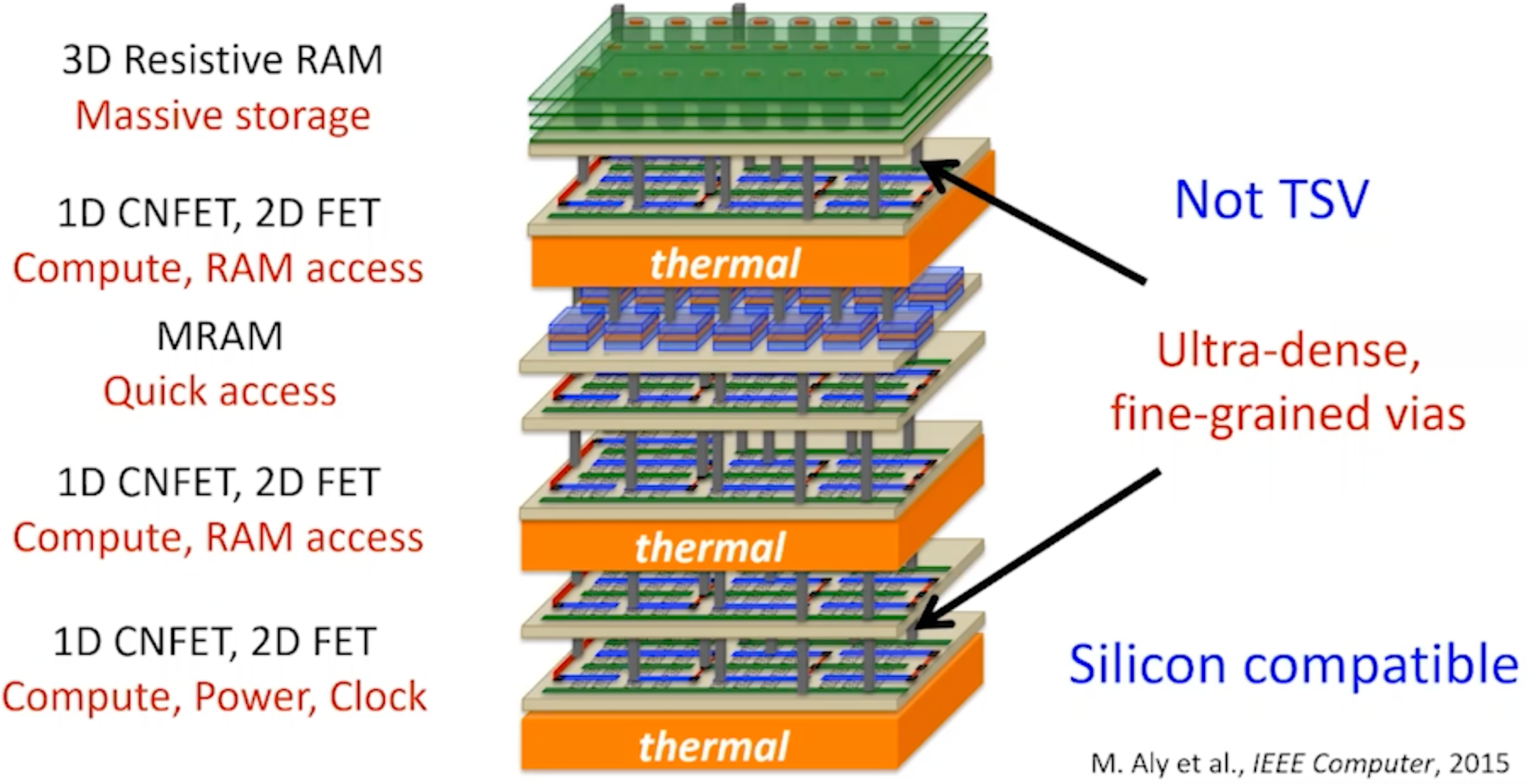
Fig. 1: TSMC’s stacked die approach. Source: TSMC/DAC
In effect, layout across multiple dimensions coupled with high-speed inteconnects can be used to balance those inconsistencies. So rather than building margin into processes, that margin shifts left into the multi-dimensional layout of a multi-die system to achieve the necessary balance. This is a subtle but innovative use for interconnects, and one that certainly bears watching.
Connecting die
Another area that is driving innovation involves multiple dies in the same package. Marvell, Intel and AMD have been doing this for some time, and all of the major foundries and OSATs are working toward the same end using a chiplet approach from multiple vendors. To do that successfully requires consistent interfaces and high-speed interconnects, but it also requires the infrastructure to be able to make all of this work.
One of the big challenges in this regard is design partitioning, which adds yet another variable into already complex designs because not everything is being done in the same process technology or at the same power and performance levels as other chips.
“This is still the early days of 3D-IC, which is a mega-merger of all chips in a system,” said Matthew Hogan, product director at Mentor, a Siemens Business. “One challenge is how you validate the interfaces. We need more management techniques for doing this. On top of that, you don’t know what other chips or chiplets will be in the package. As an industry we need to understand the electrical and physical requirements.”
This also makes it difficult to test, because so far there are lots of options but little uniformity. “Typically, you’re testing the interconnect between logic and memory,” said Vivek Chikermane, distinguished engineer at Cadence. “So far, what we’ve seen is memory on top of logic, so you can do a memory test and test the interconnect between logic and memory. But we also anticipate logic on logic. With 2.5D and fan-out you can still do probing. But with a 3D stack, it’s impossible, so you need to build in the test bus access.”
While good tools exist for automating design and testing of planar die, it’s a stretch to use them for multi-die advanced packages. Moreover, different die within a package likely will age inconsistently, making it imperative to utilize some type of internal monitoring within these packages to assess the health of the individual parts over their expected lifetimes. Interconnects are a logical placement for those kinds of monitors because they can capture minute changes in electrical, thermal, and even mechanical activity.
“These are complex systems, and you’re looking for where the bottlenecks are,” said Steven Woo, a fellow and distinguished inventor at Rambus. “There are challenges with how many transistors you can put on an AI device. That could be limited.”
Understanding those limitations, and figuring out how to optimize those devices is critical. Interconnects play an important role in all of this, and choices of interconnects may have a big impact on power, performance, area and cost.
Conclusion
It doesn’t stop there, either. Interconnects span from on-chip, to die-to-die in package, chips on a board, and board-to-board, server system-to-server system, and even beyond.
“We’re going through major transitions in architecture, to accelerators and memory,” said Tirias Research’s McGregor. “It displaces both eventually. A lot of it is tied to the level of innovation in that segment and changes in system architecture. As architectures change, that’s when new interfaces get introduced.”
—Andy Patrizio contributed to this report.
Related
Interconnects Knowledge Center
Top stories, special reports, tech talk videos, blogs and white papers on Interconnects
Interconnect Challenges Grow, Tools Lag
More data, smaller devices are hitting the limits of current technology. The fix may be expensive.
Which Chip Interconnect Protocol Is Better?
Experts at the Table Part 1: CXL and CCIX are different, but it’s not always clear which is the best choice.

 |
 |
 |
|
 |
|
 |
Leave a Reply