This is far from simple, but the power/performance and latency benefits are potentially huge.

The speed of processors has increased to the point where they often are no longer the performance bottleneck for many systems. It’s now about data access.
Moving data around costs both time and power, and developers are looking for ways to reduce the distances that data has to move. That means bringing data and memory nearer to each other.
“Hard drives didn’t have enough data flow to create the bottleneck at the CPU,” said JB Baker, vice president of marketing at ScaleFlux. “With NVMe gen 3/4, there’s so much data you can throw at the CPU that now we have this bottleneck.”
In addition, processing tasks for many compute-intensive applications like machine learning (ML) are relatively modest, but frequent. “What we all see now is that the data movement is the limiter. The computation is smaller and simpler, so it makes sense to move the data closer to memory,” said Steven Woo, fellow and distinguished inventor at Rambus.
Each of the several ways to solve this has specific applications that benefit the most. Approaches involve SRAM, DRAM, and storage, and they’re very different from each other.
Making sense of this requires clarifying terminology that’s obvious to those closely involved with memory development, but less so for others. The distinction between “memory” and “storage” can be confusing because storage is built using memory technology. (For the purposes of this discussion, “memory” refers to easily accessed working memory — DRAM and SRAM.)
Some say that the so-called “memory wall” that’s of concern to ML developers is not about memory, but about storage. “Latency between memory and computing is not the main issue,” said Marc Staimer, an analyst and principal at Dragon Slayer Consulting. “It’s the paging, at the end of the day.” If that’s the case, then the challenge lies in shortening that access time and reducing the power needed to acquire the data.
The other distinction we need involves two similar terms: “near-memory computing” and “in-memory computing.” The latter typically refers to efforts to use analog memories as a means of implementing multiply-accumulate (MAC) functions within a memory. That will not be the topic of this discussion. The focus will be on bringing computing power and data closer together, even as they remain separate.
There are two ways of bringing these resources into closer proximity — move data closer to the processor or move processing closer to the data. The architectures are similar at a high level in that, regardless of the approach is taken, the “thing” that has moved is usually smaller. So if data moves closer to the processor, you have a full-strength processor with a nominal amount of local memory. If it’s the processor that moves, you have storage for lots of data, with modest processing power nearby.
Different approaches for different memories
The three main categories of memory technologies are SRAM, DRAM, and non-volatile memory (NVM). Very different things are being done with all three.
Some note that SRAM in the form of cache is the oldest way of bringing data closer to the processor. “Near-memory computing isn’t really such a new idea — that’s what all the cache levels are,” said Gideon Intrater, CTO of Adesto Technologies. It reduces the latency for accessing frequently used data. But it also has a very specific structure that limits its use to anything but caching. “If there were a simple way to use a cache for AI, we wouldn’t be having this conversation,” he added.
Of more interest in this context is the increase in the use of tightly coupled memories (TCM). These are blocks of SRAM that are directly accessible by the processor without having to share a memory bus when doing so. The way TCM is used is completely open to the developer and the needs of a specific application. “[Today’s] dice are packed with memory [SRAM] and computing,” said Ron Lowman, strategic marketing manager for IP at Synopsys.
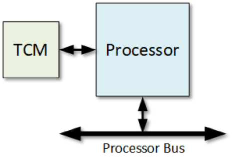
Fig. 1: A tightly coupled memory attaches directly to the processor rather than going through the standard bus. Source: Bryon Moyer/Semiconductor Engineering
This is spurring continued development of better SRAM. “We’re exploring latch-based vs. traditional SRAM,” said Lowman. “And we’ve been customizing SRAM cells for density or leakage.”
DRAM’s involvement in this discussion revolves around the one commercial approach taken by UPMEM. “I’m fascinated to see what UPMEM has done,” observed Woo. “They’re the most extreme.”
UPMEM has added a small processor to DRAM chips so that you have DRAM and processing power on the same chip. “They [the AI guys] do want the DRAM to help with the computing,” said Omar Ma, DRAM marketing manager at Winbond.
The DRAM process is not optimized for high-speed computing. It’s assumed that such processors will have dedicated chips created on a leading-edge logic process, leaving the DRAM free to use a process optimized for DRAM on separate memory chips. “The challenge has been the DRAM processes. You don’t want them to leak at all. That will make the transistors run more slowly; you can’t build the most complex cores,” noted Woo.
Therefore, the processor that UPMEM has put on the DRAM chip is necessarily under-powered, with a more limited instruction set than one would find on a standard processor. But its claim is that, even if this scheme is slower than the main processor, you can still get a performance boost because:

Fig. 2: UPMEM’s approach puts a limited processor on the same chip as the DRAM. Source: Bryon Moyer/Semiconductor Engineering
This approach has yet to demonstrate success. It must overcome a few challenges. The main one is the fact that programs must be written differently to take advantage of this. The second concern gets to the fact that you now have a chip with space dedicated to something other than memory.
“The other half of the challenge is that you need room for the processor,” said Woo. “Is the loss of memory worth the additional computing?”
This gets directly to the value one perceives in having that computing resource close by.
Computational storage
With NVM, we enter a whole different realm — a new fledgling category. In this case, we’re talking about storage, so it’s farther away from the processing and is accessed by drive-like interfaces or bus protocols, such as PCIe and NVMe. It’s effectively a solid-state drive (SSD) with added processing power.
“It has tremendous implications beyond what people think of as storage,” said Jean-Marie Brunet, senior director, product management and product engineering at Mentor, a Siemens business. “It’s a very vibrant market.”
Eli Tiomkin, chair of the Computational Storage Special Interest Group, agrees. “The state of the computational-storage market would still be classified as emerging. There are solutions available from several vendors and being used by customers.”
The memory technology being used, at least today, is flash. Other aspiring NVM technologies exist, with 3D Xpoint (phase-change) and MRAM (magnetic) memories being furthest along commercially. “They’re all coming with issues,” said Dragon Slayer Consulting’s Staimer.
But both have a hard time competing on cost. “Storage guys have been rewarded for lowering cost and adding capacity, but not for increasing performance,” said Staimer. “Intel’s is not profitable. Optane 1 was only 3X faster than NVMe Flash. The price was 5X. Optane 2 is about 4.5X faster and still 5X more expensive. You have to have at least an equal value proposition.”
Other memories, such as RRAM and NRAM, also have been investigated — with cost remaining the concern.
Computational storage devices, or CSDs, conceptually can come with different levels of functional flexibility. The simplest of them will have fixed functions, dedicating their operation to a single application. Those could be various offload functions, such as de-duplication, encryption, decryption, compression, or other similar well-defined tasks. “It’s an SSD with services built into the SSD,” said ScaleFlux’s Baker. Given how firmly these are defined, the processing could be implemented in logic rather than in software.

Fig. 3: The simplest CSD has fixed functionality, whether implemented in hard logic or software. Source: Bryon Moyer/Semiconductor Engineering
More flexibility comes if the memory contains one or more code segments, each for a different task. A main processor elsewhere could instigate the task by sending a pointer to the specific code needed at the time, or by using a custom command.

Fig. 4: A more flexible CSD may have a few functions built in, as illustrated in this conceptual view. The host then can select one of the functions, perhaps by passing a pointer or dedicated command as part of the task assignment. Source: Bryon Moyer/Semiconductor Engineering
Even more flexible would be a case where the host processor downloads the code that is to be executed. This would most easily be object code — and yet projects are also underway to download source code and implement just-in-time compilation on the CSD. That technique allows the code to remain agnostic as to the processor that will execute it.

Fig. 5: The most flexible approach to a CSD would allow the download of arbitrary code, either in object or source format, as shown in this conceptual view. If source code is downloaded, then the processor would need to support just-in-time compilation. Source: Bryon Moyer/Semiconductor Engineering
Staimer also cautions that there are two levels of computational storage — systems and drives. What we’ve been discussing is best described as a drive. It’s a single board that looks like a drive and happens to have computing capability. “For most people, when you use computational storage, that means you’re putting a CPU on a drive. This isn’t the only way to do things,” he said.
A system might consist of a number of drives, and each drive could have computation, or they could be standard drives with a single computing resource. The only commercial example of a system today is Oracle’s Exadata offering, said Staimer. “The relevance for most computational storage will be at the system level, not at the drive level. Even if there are drives, it will be a system vendor that does the integration,” he said.
The interfaces for these CSDs are not cast in concrete yet. Right now, PCIe and NVMe predominate. Some think CSX possibly could have a role. Arm’s view is that Ethernet would be easier yet, because PCIe has bottlenecks and the PCIe roots are expensive. “With Ethernet, you can scale more easily,” said Neil Werdmuller, director of storage solutions, automotive and IoT at Arm.
In addition, no standard commands exist for pointing to code on the drive, or for downloading object or source code. If such applications prove viable, standard interfaces would make this more accessible to a wider range of developers. “There are systems in the market, but they’re proprietary,” said Intrater.
Infineon is one example of a company doing proprietary CSD. “We’re doing a large amount of flash with a small processor,” said Sandeep Krishnegowda, senior director of marketing and applications, memory solutions at Infineon. But customers can’t develop directly on it. They work with Infineon to define custom commands.
The Storage Networking Industry Association (SNIA) currently is working to define the inter-workings and intercommunication for CSDs. “The Computational Storage [working group] has developed a path to define three variants of computational storage,” said Tiomkin, who also serves as vice president of business development at NGD Systems. “These include a CSD (Computational Storage Drive), which is a single SSD form factor with … a monolithic ASIC, as shown by NGD Systems, an FPGA implementation, as shown by ScaleFlux, [or] even an FPGA + SSD ASIC, by Samsung. There are also computational storage processors (CSPs) that are on the storage plane, but not tied directly to storage media, as shown by Eideticom. Finally, we have computational storage arrays (CSAs) that are a system level solution, of which we do not have a pure example today.”
The FPGA and custom ASICs dominate. “Right now we see a lot of computational storage handled with an FPGA or custom ASICs,” said Baker. Using an FPGA helps designers to experiment with new applications and services. “Over time, there will be services to be hardened into an ASIC.” These are board-level products, so the processors, FPGAs, and memories each can be built on an optimal process.

Fig. 6: Four CSD architecture alternatives. Source: SNIA
The different use cases also suggest this software would be harder to program than a typical application. Memory management would operate differently, and a host program would need to schedule tasks on the CSD — details that operate on a level lower than what most developers want to deal with. “There are more application developers than deeply embedded programmers,” said Arm’s Werdmuller. “People want to write in a higher-level language than C.”
“If you have a program where some code executes in the CPU and some in memory, you have to think that through,” said Rambus’ Woo. “Maybe over time there will be libraries and layers of abstraction.”
Added Staimer: “Some vendors have opened their storage systems for use with VMs and containers, but this didn’t sell well, since it’s too hard to write distributed code.”
If FPGAs are used, hardware design also would be required. In most cases, these are skills that aren’t traditional within the storage community.
These skill-set issues lead to a number of approaches to CSD offerings. Some provide an open environment that a customer can use to build applications. But given the likely customers, Staimer said you must have a well-defined application or suite of applications and sell at that level. Rather than selling a CSD, you’re selling a set of micro-services. ScaleFlux uses this approach: their customers can’t change the internal program; they’re buying specific services.
Greater capability comes from Linux. “If you run Linux on the drive, you basically have a nano-server,” said Werdmuller. It can be managed with standard hosts, and everyone can write applications for it.
This also lets the system be smarter about the data.
“Storage today has no idea what the data is,” said Woo. “If you compute on the memory device, you need semantic awareness.”
With Linux, you can define a file system, and the system can be more intelligent about whether a file is an image or a sound file or some other type of data. That capability will elude some current systems. “Many of these drives use Cortex-R-like processors — they can’t do Linux,” noted Werdmuller.
CSD integration
Integration roadmaps are less clear for CSDs. If you want lots of storage, you’ll likely remain at the board level because that provides room for more data. Smaller boards using the Universal Flash Storage (UFS) standard also could plug into systems designed for that format. “Board-level is easier thermally,” said Woo, noting that processors produce a lot of heat and memories don’t like to get hot.
The next level of integration would place multiple chips in a single advanced package. Here again, one can use memories, logic, and processors developed on optimized processes. The tradeoff would be that you can’t put as much memory inside a package as you can on a larger board. “If you want a lot of storage and a little compute, then stacking [memory chips] wouldn’t make sense. But if it’s more balanced, then stacking might make sense,” noted Woo.
The highest level of integration would come from putting the pieces together on a single chip, for a monolithic solution. This immediately poses the challenge that you can no longer use an optimized process for each portion of the system. Compromises will be necessary. Novel NVM technologies have the expected benefit of being more compatible with CMOS processes than flash memory is, so their emergence could make such integration easier if the density and the cost permit.
Co-packaging and monolithic integration may appear challenging, but that hasn’t stopped this trend. “We see both happening,” said Mentor’s Brunet. Not integrating helps to prove out the strength of a technology, and, in these early days, integration is not likely. In the long term, it’s reasonable to expect a push to integrate for space and cost purposes.
CSD design and verification are tougher than what’s required for a simpler SSD. SSDs usually are verified using in-circuit emulation, or ICE, which involves implementing the design on an emulator and then feeding data through a physical connection with a data source. That means someone needs to establish that physical connection, and data speeds may need to be adapted to work with the slower verification system.
With CSDs, you have to validate the computing as well. ICE no longer works well here. Everything is virtualized, including the data sources.
“This is accelerating the ability to do pre-silicon measurement that can’t be done with SSD/ICE,” said Brunet. Because of the wide range of possible applications, the emulator will need to be able to boot Linux (for CSDs that support it) and run the various service applications that the CSD is intended to support.
CSD applications
CSD applications vary — and yet they’re similar in character. Some of them work on data and return an answer. Others pre-process data before sending data so that the quality of returned data is higher, with the “garbage” eliminated.
Application examples include:
But again, the application is key. “It’s going to be application-driven,” said Stamier. “It’s not going to be, ‘Here’s a better mousetrap, come buy it. The fact that it’s a CSD may be a curiosity, but the real value is in the services provided.” He suggests that CSDs offered up for others to program are not likely to be successful.
Conclusion
All of the near-memory examples we’ve looked at — with the exception of TCMs — are in early days. That means further evolution is likely.
“The market is moving extremely quickly,” said Synopsys’s Lowman. “It’s a really exciting market. The technologies continue to leap-frog each other.”
 |
|
 |
 |
 |  |
 |  |
3DSoC.
And before that, 1 GB or more L4 cache on the I/O die with AMD Zen 4/5.
The energy cost of going to DRAM is 200x that of on-chip memory and the latency is horrible, it’s just going to disappear – NVM technologies like Optane will replace it in the above mentioned 3D-SoCs, along with stuff like asynchronous logic to get the power down.