Data analytics is quickly becoming an indispensable part of the complete IC production flow.

Single die packages and products have been the norm for decades. Moreover, so has multi-chip modules (MCMs) or system in package (SiP) for quite some time. Understandably, with ASICs and SoCs becoming larger while silicon geometries continue to get smaller, there is an opportunity to combine even more functionality into a smaller form factor for the end product. Hence, new advancements in design continue to surface as can be seen by the advent of new chiplet-based design and architecture and advancements in packaging as seen in the latest 3D-IC packages.
While advancements in design and packaging continue to track with the advancements in silicon processes, the complexity and costs in the manufacturing and testing of these new state-of-the-art devices also continue to grow at a large rate with significantly more data being produced daily. Intuitively, you can imagine today there are more expensive packages and overall more thorough tests needed than ever before. If that were not daunting enough, there is now even more pressure to ensure high yield from each of the individual die or chiplet hosted within each MCM package or multi-chiplet package as it only takes one failed die or chiplet for the whole device to fail.
The methodology described in this article for the debug and traceability throughout the manufacturing test process of these devices is the same regardless of whether we discuss traditional MCM designs or the latest multiple chiplet designs placed in either SiP, 2.5D-IC or 3D-IC packages. Therefore, for the remainder of this article, I will be generically referring to MCMs as the packaged device under test and dice to represent the chips within the packages for simplicity.
It is important to understand the different test stages as literally failures can occur at any stage. The later the systematic failures occur, the more costly it is for the company to develop these devices due to the wasted tester time spent testing these ultimately failed devices. There is also the lost revenue and costs associated with manufacturing these dice and the associated costs if these dice make it into a package before failing.

Fig. 1: Stages of manufacturing test.
The predominant Manufacturing Test stages shown in figure 1 are Wafer Acceptance Testing (WAT), BUMP, Wafer Sort (WS), Assembly (ASSY), Final Test (FT) and System-Level Test (SLT). One costly scenario would be if the device makes it to FT or SLT after having been assembled into an expensive MCM package only to see them fail at a high rate.
For example, suppose you do happen to begin experiencing significant yield loss at FT or SLT. In that case, it is imperative that you correctly identify the source of the excursion and rectify the problem as soon as possible. One logical place to look is in the ASSY process since the dice in the MCM package are each perceived to be known good die at the time of assembly as each die had previously gone through rigorous testing in prior test stages and passed. However, it could also very well be that specific attributes introduced into the design or package of the MCM or perhaps the new test requirements at this later product stage may now prevent certain dice from passing FT or SLT. But where do you begin to troubleshoot and find the source of the problem? The answer lies somewhere in the data.
To find the root cause, you need a way to trace the life of each die within each failed MCM back through the various manufacturing test stages. The process, also known as data feed backward, is depicted in figure 2 below. At this point, your task is really to see if there is a test parameter or fab condition from an earlier stage in the manufacturing process that can predict failures you are now encountering during ASSY, FT or SLT. Doing so will enable you to rectify the problem earlier in the process and prevent future failures during later stages, saving you a lot in expensive manufacturing packaging and test costs. A process known as data feed forward is also shown in figure 2.

Fig. 2: End-to-end part-level and MCM-level traceability and correction.
To properly be able to trace the life of each die requires at least three things.
In this real-world example, a company was developing a 4-die MCM packaged product and was experiencing failures of their MCMs during FT which resulted in 84% yield, as shown here in the failure Pareto chart in figure 3. This did not quite meet their targeted yield requirement for their MCM product and therefore, they needed to debug and fix the problem as soon as possible. From the failed bin analysis, it was evident that the majority of their FT failures were coming from Bin 6 which were the functional test failures.

Fig. 3: Failed bin Pareto chart.
The next thing they wanted to see was the FT failed bin results superimposed back onto a wafer map to check if there happens to be any geospatial relationship between these bin failure types and the location of where the dice originated from on their respected wafers before placed into their current MCM package. The wafer map shown in figure 4 interestingly reveals that the dice within the failed Bin 6 packages predominantly came from the center of the wafer map.

Fig. 4: ECID maps link the FT result back to the source die X/Y location.
Notice that each die in a given MCM were selected from the same wafer. This tells you that all four die are the same design replicated four times within the MCM. Another interesting finding was that the dice selected for each MCM product came from the general vicinity within the same wafer. Generally speaking, no requirement suggests that all dice within a specific MCM originate either in close proximity of each other or even come from the same wafer. It so happens that this company chose to select their dice within the same wafer area for each MCM device. This could be due to perceived similar performance selecting dice from the same area or perhaps also simplicity or convenience in selecting the dice that go together into an MCM package to aid in the ASSY process.
One other important finding is that it appears, but not guaranteed, that only dice related to this particular MCM product are represented on this wafer map in figure 4 instead of other MCM products of the different number of dice or possibly a single die product coming from this same wafer. Further, notice what you see around the orange-colored dice depicting the Bin 6 failures. The surrounding dice are “grey” in color. This can mean any number of things but typically one of the following:
However, seeing how many orange dice are failing FT from the same area, you may rightfully be thinking that perhaps these other surrounding grey-colored dice are either borderline bad die still somewhere in production or they previously failed during WS testing and were already binned out. Hence, if in fact these grey dice failed sometime during WS then you would be witnessing the classic pattern of Good Die Bad Neighborhood (GDBN), where if proper quality measures were previously taken, you would want to “ink out” those neighboring good dice (colored in orange) prior to having them selected and assembled into this MCM product. Thus, many of the orange-colored dice should not have been given a chance to continue in the manufacturing process and been placed into the MCM product if proper quality measures had been put in place.
To be certain, let’s take a closer look at how this particular wafer performed during WS. We are expecting to see some center pattern of failed dice if our assumption of GDBN holds true. Figure 5 below shows the composite view of all WS tests results performed on the dice within this wafer map. But wait, where is the center pattern of failed dice? This discards any notion of GDBN since most of the dice in the center of the wafer passed all of their respective WS tests (denoted by the dice shaded in white). Therefore, these good dice at the center of the wafer did not fail WS. This means that these corresponding good dice that were also shown to be grey in the previous map in figure 4 containing the FT results either have not been tested yet if they belong to the same MCM product or they were put into a different product altogether that is not shown.
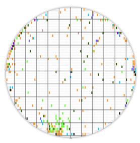
Fig. 5: All WS bin results for this wafer.
So, at this point you might be wondering, what other options do we have to find the source of the problem? Well, we can start to look into the tests performed during the assembly of these specific MCMs that are failing. We can also continue to look to see if there are any WS parameters that have a similar pattern to the orange colored center die pattern of the failed MCMs during FT. But which parametric tests during WS should we try to correlate the FT failed bin map to? This is where the power of a good data analytics solution comes in very handy.
The company in this case simply selects an option to automatically have the tool correlate between all WS parametric test results and the FT ECID module failed binning results. Here in figure 6 below is what the tool came back with, along with the following graph in figure 7 showing the measured WS parametric results of a specific leakage current test of the failed dice identified at FT.

Fig. 6: Correlation results across all WS parametric tests and FT ECID module binning results identifies a matching pattern from one parametric test.

Fig. 7: WS Leakage Current parametric test results of the failed dice from FT.
The tool came back saying it had found a match! In looking at both wafer maps above, there is an apparent match in terms of a specific pattern of activity affecting the center of both wafers. The color scheme shown in the WS Leakage wafer map indicates the wafer is “cold” in the center and radially increases in temperature as it goes outward towards the outer edge of the wafer. The wafer is not actually cold in the center. The term cold is often used to describe very low leakage which can also correlate to slower performing devices. The performance should improve for the other devices as you move towards the outer regions of the wafer. However, hot devices are not necessarily better. While hotter devices may operate at faster frequency, they also have higher leakage current and will have a shorter battery life. So, depending on the application, the sweet spot might end up being somewhere in the middle between cold and hot in order to achieve the desired power/performance balance for the device.
It is clear that low leakage results shown at WS is causing the FT module fails in Bin 6. The numbers on the X-axis are current measurements in milliamps. As mentioned, low leakage devices are good for drawing very low power and generating longer-lasting battery life. However, the most prominent issue in this real-world example is the dice at wafer center are simply performing too slow and are likely not meeting the MCM specification. To be precise, since there were 292 dice that made up all of the Bin 6 failed MCMs, then a total of 73 MCMs (292 / 4 = 73) from this wafer alone had failed FT and had to be either scrapped or potentially relegated to be sold at a lower price point for an end application not requiring fast performing devices.
But what steps can be taken now to prevent having many more of these costly failures at FT? Taking a closer look at the graph in figure 7, it appears that the lower spec limit for this test was set to zero while the upper limit was set to 16 mA due to the red lines depicting the spec limits. A straightforward solution would be to simply move the lower spec limit to the right such that future dice that measure outside to the left of this new lower limit will fail this WS Current Leakage test and get binned out earlier in the process. The question then becomes how far to the right do you want to move the lower spec limit? Would you move it to 0.5 mA, 1.0 mA or maybe even 1.5 mA? The answer lies within the cost-profit tradeoff analysis between how much you sell these MCM devices for versus how much it costs to build each MCM device.
But wait, there is more to consider before you decide to move the spec limit and by how much. Thus far, the analysis shown was only on one wafer; hardly a representative sampling of the entire production line of products being produced. Is making a decision as significant as moving a spec limit that may bin out potentially a lot of good dice a good idea after only analyzing one wafer? The answer is obviously not. Unfortunately, the full production data for this MCM product was no longer available when we decided to write this article. However, the next logical step in our real-life example would have been to move up the level of scope to encompass all manufactured MCMs to date and perform a similar FT Bin vs WS Leakage plot as shown above but now against the entire MCM population instead of on only one wafer.
Assuming after analyzing the entire MCM population, you determine that all failing devices at FT are not usable and if by moving the spec limit on this one test during WS you are mainly catching those dice that are causing FT failures while also not throwing away any good dice, then your profit margin should definitely increase by binning out the bad dice earlier during WS. The main reason is that you are saving on the build costs by not moving those bad die into expensive packages. A good data analytics solution would allow you to manually drag the spec limit to simulate the net effect of how many dice you would lose during WS if you moved the limit. This simulation will allow you to assess the tradeoff between your collective costs and profitability at FT.
The real-life example described in this article could have been an extremely costly problem for this company if it were not for the data analytics solution used being able to quickly isolate the issue within a matter of minutes. The ability to trace the history of every die within every failed MCM as well as the ability to correlate every test ever performed on those dice at the push of a button was paramount in being able to quickly resolve this potential economic hardship. But was this the worst-case scenario? The answer is no. Something worse could have transpired.
The biggest concern for any company is that their manufactured devices eventually go into the designated end product, sold to the end user, and fails while in use. The company will not only suffer potential future business loss but may also suffer irreparable damage to their brand reputation. Taking the severity to another level, what if the device eventually was used in an automotive, transportation, or medical device application where a defective device may result in a loss of life? This would likely be the worst-case scenario you would want to avoid at all costs. Ensuring high-quality devices was not the focus of this article. However, ensuring high-quality devices is something a good data analytics solution can deliver on by instituting several different types of outlier detection and escape prevention techniques to ensure that only the highest quality devices ever get manufactured and deployed in the end product.
What course of action can a company take if their devices start to fail beyond an acceptable threshold while in use in the field? The answer again lies within the manufacturing test data. As devices start to eventually get returned as Return Merchandise Authorizations (RMAs), analysis can quickly be performed on these returned devices by first identifying the unique ECID or 2D code in each device. From there, you can start to bring up the entire history of test data results on each die within each device. You would then similarly start to run analytics on all of the data if it has not already been done before and have the tool identify any potential issues it may have found in analyzing and cross-correlating against all of the test data.
The ultimate goal in analyzing RMAs is twofold: (1) Identify the source of the problem and correct it so that future manufactured devices will no longer have the same problem and later fail while in use, (2) Proactively look for “like” devices that tested similarly to those that were returned as an RMA but are still in use in the field. Depending on the severity of the problem, the company may actively want to “recall” specific outstanding devices identified by their ECID or 2D code that can be traced into the end product actively in use by tracing the corresponding part serial numbers in the supply chain until the questionable end products have been identified and securely recalled.
Of course, not all of these corrective actions are possible to incorporate without the right data analytics solution.
Unfortunately, not all data analytics solutions in the market today solve problems in the same way or with laser-like timing and precision. While there is potential that most or all solutions may ultimately derive at the same conclusion, the difference comes in how fast it takes to find the root cause and institute a corrective action to correct the problem.
When evaluating data analytics solutions, here are certain attributes that you may want to look for:
The product used in this real-world example is called SiliconDash from Synopsys. Please visit us on our website for more information on this indispensable technology and watch our recent webinar available now on-demand featuring a live demonstration and a keynote presentation from Marvell explaining the benefits of a big data analytics solution that was finally architected correctly.
 |
 |
 |
 |
 |
 |
 |
Leave a Reply