Why balancing the costs of semiconductor test and reliability is increasingly difficult.

Balancing reliability against cost is becoming more difficult for semiconductor test, as chip complexity increases and devices become more domain-specific.
Tests need to be efficient and effective without breaking the bank, while also ensuring chips are of sufficient quality for their specific application. The problem is that every new IC device adds its own set of challenges, from smaller features and new materials, to the integration with discrete components such as chiplets and entirely new technologies such as backside power delivery. Test probes need to be designed for smaller batches of wafers, and more advanced (and expensive) equipment is needed to examine each part and make sure it will work as expected.
“There’s this constant balance that has to occur,” says Keith Schaub, vice president of technology and strategy at Advantest. “We need to apply the budget to get as much test coverage as we can at the best quality for that budget. That’s where the challenge is.”
That challenge is even greater in safety- and mission-critical markets, where a glitch can have serious consequences. In fact, a defect in most of today’s high-growth markets is more than an inconvenience. Shorter test times may be a key way to keep costs in check, but they come at the expense of a device’s reliability. On the other hand, the more thorough the testing, the higher the chances to identify all failures. The catch is that the deeper you go with testing, the more time it takes, which in turn increases costs.
“One approach to reduce these costs is to deploy deep data algorithmic techniques or ML for ‘dynamic testing’, which considers each chip’s individual DNA based on chip telemetry,” says Alex Burlak, vice president of Test & Analytics at proteanTecs. “This method alternates the test flow dynamically by identifying each chip’s unique process signature and not executing a ‘static’ flow for all ICs.”
The cost of quality
CapEx and direct expenses of testing are only one aspect of quality-related costs. For a manufacturer, a failed chip means a loss in materials, time, and the energy taken to produce it. And if a defective chip makes it to market, the stakes are many times higher.

Fig. 1: Identifying potential field failures and test issues are critical for quality assurance. Source: Bruker
A latent defect, for example, can lead to a product failure when the chip is in use, potentially resulting in expensive recalls, repair costs, or even charge-backs from the customer, depending on the application of the chip. These scenarios can cost the manufacturer significantly more than the value of the chip itself.
“What are the costs of defects? What does it actually cost if something fails at final product?” asks Frank Chen, director of applications and product management at Bruker Nano Surfaces and Metrology. “Some manufacturers think it’s just the material scrap cost from lower yields. They don’t think about how much it costs their customer if marginal defects pass through and fail later. That can be 10 times or 100 times more expensive than the material scrap cost.”
This domino effect of failures in the field can be much more costly than just additional tests or scrapping a marginal part. A common assumption is that budget constraints guide the level of quality. While that is true in many cases, what’s less obvious is that quality also determines costs.
“The prime motivation is quality,” says Mark Kahwati, product marketing director in Teradyne‘s semiconductor testing group. “You know what’s at stake when a test escape happens, and what device performance you are trying to guarantee to your end customer. How much test do you need to ensure quality-level objectives are met?”
The relationship between quality and cost in semiconductor manufacturing is cyclical, not linear. The drive for quality defines the needs for tests, and the amount of testing and number of insertions drives the costs. As those costs start squeezing an already narrow profit margin, there is pressure to cut those costs, which then can impact quality.
“We’re constantly trying to reduce the cost, but not necessarily to save money,” says Schaub. “It’s usually to improve quality. It’s not so much that cost dictates the amount of testing to achieve quality. It’s that quality drives the necessity for tests, and cost is the consequence.”
New models needed
The well-known triangle model of yield, quality, and cost has served as a longstanding barometer for production decisions. Yet in today’s landscape, where chips are destined for a variety of applications, many with different levels of criticality, this old model needs some tweaking.
Yield is where the profit lies. The more sellable chips you can get out of a single wafer, the lower the average cost per part and the higher the margin. But just focusing on yield is insufficient. Quality increasingly is viewed as more important these days, but not always, because that depends heavily on the application and use case. What is considered high quality for one use case might not suffice for another. The testing protocols for a chip in a medical device, for example, are much more stringent than those for a chip designed for a household appliance, and the higher selling price may compensate for lower yield.
Testing itself has evolved to reach far beyond the confines of the fabrication facility, as well, extending into the functional lifespan of the device. Customers today increasingly require continuous monitoring or silicon lifecycle management (SLM), which tracks a chip’s performance and identifies signs of aging or degradation over time. This level of monitoring is essential for components critical to systems where safety is paramount, and it adds to the chip’s complexity and expands its costs over time.
The challenge lies in dynamically adjusting the testing approach during manufacture without compromising the integrity of the final product. It’s a delicate dance between ensuring safety, maintaining performance standards, and doing so within tight testing budgets. With the addition of SLM, the commitment to quality extends into an ongoing responsibility that goes beyond shipment and continues throughout the chip’s active duty.
In essence, each vertex of yield, quality, and cost triangle must be evaluated in the context of increasing complexity. The true cost of quality is a measure of resources spent, the value delivered to the customer, and the potential liability for failed parts. Manufacturers must not only balance cost versus quality, but also predict the unknown and factor that into their profit equations.
“Whenever the cost of non-quality exceeds a certain threshold, customers are ready to invest in metrology and quality control so their yield goals are achieved,” says Samuel Lesko, senior director and general manager at Bruker Nano Surfaces and Metrology. “On some occasions, like advanced packaging, the yield is directly linked to the metrology data you get out, so there is no process without it. Metrology becomes part of the process where the information collected in quality control feeds the next process step.”
Manufacturers are also utilizing their high-CapEx equipment across a greater number of insertion points to get more volume out of the same equipment and streamline the processes.
“One way to save is through scaling,” says Lesko. “You want interoperability, so the system is not dedicated to one product line, but is shared across the whole range of product lines. Whenever you have to add multiple sensors to your tools to get all the measurements, the costs will increase. If you can, use a single measurement head or sensor that is robust enough to accurately capture all the requirements. Quality cost drops through minimizing idle time and increase of productivity.”
New challenges emerge
When new products are designed, the number one goal is getting them to market on time. If a company like Apple or Samsung is introducing a new mobile phone in time for the holiday shopping season, there is no scenario in which chips can be delayed.
“You can’t miss that window,” says Schaub. “That drives everything. But often your test programs are not optimized because you have to hit the window, and that can impact the quality of the chips that get shipped with the devices, where the cost of failure is much higher. It could be, as a manufacturer, that you want to increase that test budget up front to decrease those failures down the road. I don’t know exactly how they allocate the resources to do that, but that is a big challenge for manufacturers now.”
Additional costs that must be factored in are potential returns, and in some cases penalties imposed by the customer when a chip is identified as the culprit in product malfunctions. Those costs can amount to several hundreds or thousands of dollars per failure, depending on the application.
“One method to complete this cost-of-defect feedback loop is to penalize the manufacturer for each failed part,” says Chen. “If a customer determines that it’s your chip that caused a failure in their product, they will apply a fine for the price of the finished product. That puts a hard line on the dollar value for what it costs when there’s a failure.”
DFT versus physical test
One avenue for reducing test costs while maintaining quality is an increased emphasis on design for test (DFT). DFT can lay the groundwork for more streamlined testing during production and helps reduce costs through the early detection of potential faults with advanced simulations and built-in test logic.
By simulating various fault scenarios and stressing the digital twin models of the designed chips, manufacturers can predict how a chip will behave under specific conditions. If the models indicate potential fault points, engineers then can introduce optimizations in the manufacturing process to mitigate these issues, which can range from changes in die layouts to adjustments in the fabrication process itself.
“Many early simulations can be run through the various tools, where you can gain some predictive insight about where you think there’s going to be a problem,” says Travis Brist, senior product marketing manager at Synopsys. “That insight can help account for those problems in advance and set up specific tests where you bury certain parameters to see, ‘Okay, how sensitive is it to some of these things that we suspect will be a problem?'”
This is essentially a way of raising the abstraction level to identify potential problems more quickly. “How can we make the best use of all this data that’s coming in,” says Brist. “There’s so much data out there, and it’s impossible for a person to look at it and try to discern anything. They might find some little problem, but it might not show the big picture of what’s happening.”
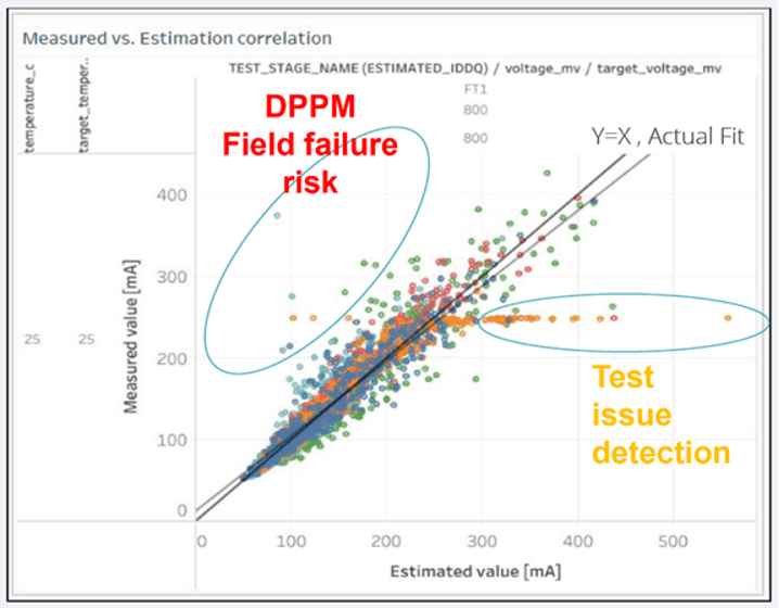
Fig. 2: Personalized outlier detection compares actual IDDQ with predicted IDDQ per chip. Source: proteanTecs
“DFT is not a luxury,” says Teradyne’s Kahwati. “It’s a must-have that continues to evolve and help provide economically strategic test coverage decisions that happen before the device is even fabricated.”
Engineers use DFT to offload some testing complexity and cost, but it cannot cover all aspects, especially as chips become increasingly heterogeneous and disaggregated. High-speed interfaces, for example, may still require expensive ATE to confirm performance. Moreover, while DFT excels in logic-centric testing, other areas like analog and RF require more traditional testing techniques to ensure comprehensive coverage. Physical testing, while more cumbersome than simulations, offers the irreplaceable benefit of certainty.
“There are two obvious areas where DFT helps with test coverage,” adds Kahwati. “One is scan testing, or logic testing. The other is loop back. If you think about high speed PHYs, those are really difficult and expensive to test with ATE, and always have been. So the extent that DFT can have test IP, or loop back capability, can help mitigate rising test costs while providing adequate levels of coverage.”
Even though DFT can help reduce test costs, it’s a logic-centric process with limits. DFT may not have access to all interfaces, and there may be interactions between different die or different transistor types in multi-chip/chiplet devices. It’s also ineffective with analog/RF blocks.
“DFT is good for built-in self test and scan chains,” says Advantest’s Schaub. “That enhances the testability of devices, especially the digital ones, but it does have limitations because it doesn’t cover all the device aspects. It misses analog characteristics, and it doesn’t provide long-term reliability. So you can’t tell how it’s going to perform over time, which is critical for a lot of the new medical and automotive applications. You still need some comprehensive system-level testing to understand how it’s actually going to perform in real life scenarios.”
The key is finding the optimal intersection of DFT and physical testing. While DFT can cover a wide range of potential issues and reduce test costs, it must be balanced with the lowest level of physical testing required for quality assurance. Given the variability and unpredictability of chip performance, especially in multi-chip and highly integrated devices, manufacturers must continually adapt these strategies.
“In-line inspection and metrology work alongside DFT with good correlation to electrical tests, but we’re getting that information at a much earlier stage,” says Bruker’s Chen. “That’s already valuable because you get earlier screening as well as physical parameters from the process. The next level of confidence that we’re working towards is active process feedback based on these measurements.”
Test time reduction
DFT can help maintain a balance between quality and test costs, but it’s not a panacea. The subtleties of device interactions, the necessity for tests that emulate operational conditions, and the diversity of chip applications necessitate a blend of both DFT and physical testing. Engineers must make strategic decisions on the depth of DFT to implement and when to lean on the certainties of physical testing, all while considering the end-to-end test costs and the absolute demand for quality.
This is where test time reduction (TTR) strategies come into play. By embracing TTR, companies can streamline their testing procedures, reducing time and associated costs without lowering the bar on quality.
“While enhanced DFT coverage is critical, it is geared more towards ATE test stages and does not provide parametric visibility,” says proteanTecs’ Burlak. “It is limited to pass/fail decisions. This approach misses the detection of potential ‘walking-wounded/anomalies, in which the chip passes but will fail later in the field, resulting in expensive service disruptions.”
Another approach is test time reduction. “When you’re trying to ship a new chip, you go through the test optimization cycle, but that can last for several weeks or months with teams around the globe working to reduce that time and cost,” says Schaub. “It’s what we call TTR, and that’s been in the industry for the past 20 years. It’s a big hammer that can really drive down the cost of testing.”
The complexity of today’s semiconductor devices often warrants thousands of parametric and functional tests. While ensuring device reliability, those also result in significant usage of expensive automated test equipment (ATE). TTR can help manufacturers explore multiple methods to cut down test times, such as eliminating redundant tests, re-ordering test sequences to catch major failures early, and sampling or removing consistently passing tests. This software-assisted approach offers a more data-driven decision-making process, and a potential test time savings of 15% to 24% without affecting quality while reducing the product’s time to market. [1]
New strategies for lowering costs
As the semiconductor industry continues to advance, so does the need for strategic approaches to managing testing expenses without sacrificing quality. Parallel testing is one of the significant innovations in this area, particularly for system level test where the capital expenditure is typically higher than that for an SoC tester. High-volume manufacturing tests benefit from this approach, allowing multiple devices to be tested simultaneously, substantially driving down the cost per test.
“The parallel cost savings bonus that you get from SLT is around a factor of ten or higher than with SOC,” adds Schaub. “Your cost of test goes way down. Generally, it’s an order of magnitude less costly for system level test than wafer or package test.
Teradyne’s Kahwati agrees, especially when addressing the limits of scan bandwidth. “The number of pins available on a device can restrict scan testing, and that adds test time on a tester, which increases costs.”
To address this, the industry is exploring methods to enhance scan bandwidth, such as protocol scans over standard interfaces like PCIe and USB, as well as streaming scan networks, which aim to increase bandwidth without adding pins to the device’s package. These advancements help to alleviate bottlenecks in scan time growth while maintaining the required coverage dictated by quality goals.
Manufacturers also are utilizing their high-CapEx equipment across a greater number of insertion points to get more volume out of the same equipment and streamline the processes.
“One way to save is through scaling,” adds Bruker’s Lesko. “You want interoperability so the system is not dedicated to one product line but is shared across the whole range of product lines. Whenever you have to add multiple sensors to your tools to get all the measurements, the costs will increase. If you can use a single measurement head or sensor that is robust enough to capture everything and ensure accurate measurements, you are reducing your cost of quality by minimizing idle time and increasing productivity.”
There are other options, as well. “Enhancing test time at SLT or system testing by utilizing parametric visibility during functional workloads can enable dynamic flow control in terms of testing less or more,” says Burlak. “The building blocks to enable these strategies require an end-to-end approach with solutions that leverage on-chip monitoring IP and provides accurate process signatures and margin measurements during functional workloads.”
All of these solutions for cost management in testing are crucial as manufacturers address the increasing complexity of semiconductor devices and strive to meet critical quality standards. Each strategy, from parallel testing to integration of DFT elements like loop back capabilities, contributes to a comprehensive plan for lowering test costs while ensuring device reliability.
“The architecture of the tester is very important to the industry, because these testers are not cheap,” adds Schaub. “They are typically hundreds of thousands or millions of dollars. Customers want to be able to utilize them at a very high rate, while also addressing many market segments.”
Judicious use of available technology is the key. “The ability to port test coverage can optimize the cost of quality over the whole breadth of the manufacturing flow,” says Teradyne’s Kahwati. “Early in the manufacturing process, when the process may not be stable, you might discover a need for more coverage at wafer sort because you’re getting a lot of defects. As the process matures, your yield begins to improve, so some of that test coverage can move downstream to a system level test because it’s more economical. I think that’s a capability that will become increasingly important with these advanced process nodes, but we’re not quite there yet.”
Conclusion
The challenge of testing semiconductor chips is about managing costs while not sacrificing the quality of the product. Device makers take advantage of DFT and TTR strategies to stay within budget and maintain high standards. DFT helps find problems before they happen, while TTR focuses on making the necessary tests as quick and efficient as possible.
These methods are important because they help keep testing affordable, but they have to be used wisely. Not every problem can be predicted by DFT, and not every test can be shortened by TTR without risking missing a defect. It’s a balance that demands constant attention and adjustment. The goal is always the same — to deliver reliable chips to the market as cost-effectively as possible. This is the way manufacturers ensure they provide what customers need at a price that keeps business moving forward.
Reference
1. Addressing Test Time Challenges
Improving test strategies is key to cutting costs.
Related Reading
Improving Reliability In Chips
Experts at the Table: Tracing device quality throughout its expected lifetime.
 |
 |
 |
 |
 |
 |
 |
Leave a Reply