Maintain design integrity amid the growing complexity of the high-density fan-out package design environment.

Why should there be an interest in Package Assembly Design Kits (PADK) today? For the most part, it is due to the advancement in the accumulation of files forming the PADK now offering a customized heterogeneous design experience that optimizes the device’s intended package performance with complete connectivity verification, DRC, and assembly validation. Another primary reason is the ongoing focus on reducing the design cycle time. This is possible by beginning with clear and proven manufacturing and assembly checks that can be implemented during the initial layout phase, thereby reducing the need for rework of the design layout during post-process checking. In a blog discussing Package Assembly Kits, Paul McLellan mentions, “New challenges face both IC designers and package designers and new approaches are required.” [1] Finally, and possibly one of the most impactful reasons, is the need to maintain design integrity amid the growing demands and complexity of the high-density fan-out (HDFO) package design environment.
Electronic Design Automation (EDA) plays a major role in verifying that packaged semiconductor devices meet all manufacturing and performance requirements.
Silicon design has relied heavily on manufacturing verification through Process Design Kits (PDK). PDKs are created by foundries and provided to their customers for each of their process nodes and technology variants. The foundry customers can then use the PDKs to validate that their die designs meet the foundry’s manufacturing requirements.
Package designs have historically relied primarily on verification methods such as Design Rule Checks (DRC), Computer-Aided Design (CAD) software, and other EDA verification methods such as Computer-Aided Manufacturing (CAM). This combination of checks ensures each package design meets the intended manufacturing requirements. However, as die and package integration complexity continues to increase, so does the need to integrate die and package level verification (integration of the PDK plus Assembly DRC), forming the methodology of the Package Assembly Design Kit (PADK). High-Density Fan-Out (HDFO) packages such as SWIFT currently fall into this category and benefit from the advancements provided with PADKs.
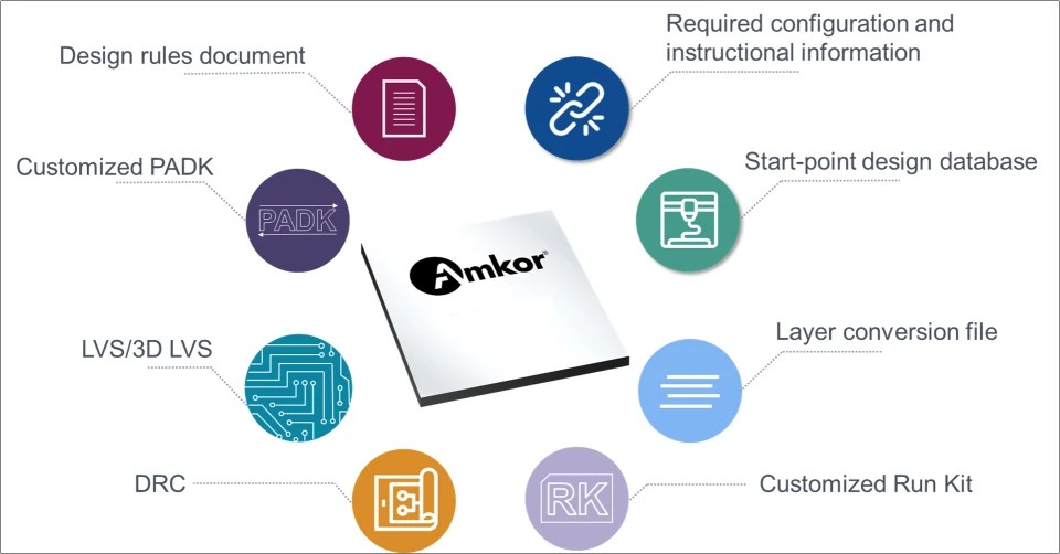
Fig. 1: Amkor Package Assembly Design Kit (PADK).
Package Assembly Design Kits replicate design rules and assembly benchmarks from the design development phase to the post-process fabrication data acceptance step. Thus, there is no guessing whether the proper design rules have been followed. The intent of the PADK technology is for the layout design engineer to utilize an easy-to-use method of verifying their design. Beginning with package feature sizes and routing guidance through to the 3D interconnections and 3D package alignment, the OSAT’s PADK provides an OEM customer the peace of mind needed to ensure complete signoff verification.
The high-density fan-out package design environment continues to increase in complexity, requiring the need for pre-approved variants of packaging technologies. These deviations in verification will meet the needs of the HDFO design layout and performance requirements. The pre-approved package technologies are built into select Run Kits. A technology Run Kit allows for application-specific variations in the manufacturing and assembly process to be agreed upon during the design phase in place of post-design acceptance. This is a very different plan compared to the simple waiver acceptance process. Waiver analysis concentrates on post-design acceptance instead of utilizing intended Run Kit variants, enabling initial design layout guidance and paving the way for the possibility of a single-pass design cycle.
Working directly with an OSAT during the development of HDFO package designs has several advantages. The first is the OSAT’s unique position as the package development, manufacturing, and assembly house. This combination enables a quick path to implementing design rules and detailed assembly requirements which are built into the PADK. Another benefit is the ability to leverage the OSAT’s experience. This experience is embedded into the Package Assembly Design Kits, thereby adding the value of manufacturing and assembly verification earlier in the package design process and reducing the number of design layout spins.
Outsourced Semiconductor Assembly and Test companies also benefit from a comprehensive partnership with OEM customers. The benefits arise from the customer enablement by saving vast amounts of back-and-forth design reviews. For example, suppose a non-optimized bump size was selected early in the design layout process. In this case, the OSAT will need to devote engineering time to determine if to accept or advise a design revision. Siemens team members John Ferguson and Tarek Ramadan shared, “While the implementation of an ADK is a non-trivial effort, both design houses and OSATs receive long-term value from the investment.” [2] The sooner items like the bump size configuration are established by the partnership and technology strategies are aligned, the better chance of a positive outcome can be achieved.
Experiencing the benefits that an HDFO Package Assembly Design Kit can provide requires allocating time and money; to what extent will greatly depend on the hardware and software currently available to the HDFO designer. However, building from an existing design workflow will help with a quick implementation process. Next, the focus is to address the following four key areas for a successful PADK implementation. The investment emphasis should go to high-end computer hardware, compatible software, advanced training, and a qualified support team.
HDFO design layout size and feature count are immense. An average design database can range from 750Mb to 1.5Gb. The number of individual items defined within the database can easily be over a million. The single-threaded processor capability and the max CPU speed measured in megahertz will significantly affect design editing and verification processing time.
Two software categories are necessary to support the design ecosystem for HDFO packages. The first is selecting the design software and verification application, and the second is the operating system environment. Major design software companies like Cadence and Siemens have specialized design layout editing and verification applications ready for the demanding HDFO design requirements. These applications, however, require the Linux operating system to support the required calculations needed to validate the fabrication data.
Educating designers on the specific software and package techniques almost goes without saying. However, the need to follow through on investing in training is vital, similar to how major sports teams spend considerable time and money to instill the most basic and advanced specialized skills within team members. This is the same requirement for technical teams. It is imperative for designers to be proficient in wafer-level design software in the Linux environment.
OSAT packaging companies are quickly developing and redefining the next-generation Package Assembly Design Kits. Wafer-level design software vendors have also aligned with OSATs and OEM customers to help continuously seek new software solutions. They are always on standby to support questions or active issues.
Package Assembly Design Kit workflows are aligned with current design software workflows or best practice design procedures. The resulting workflow is part PADK and part traditional packaging software design flow. See figure 2 below for an example OSAT focused process flow with a similar flow that can also be performed by the design layout engineers at OEM/Fabless company, made possible by the availability of Package Assembly Design Kits.

Fig. 2: Amkor HDFO Design Flow.
During the design phase, the design layout undergoes an ever-changing engineering environment, where creative solutions are tested and eventually implemented to solve complex design and electrical issues. The challenge arises when aligning the design layout with an appropriate and approved assembly and manufacturing technology. This is where the PADK becomes the technology benchmark, confirming and establishing acceptable fabrication artwork.
Lastly, the manufacturing data is comprised of many individual features, of which each need to be checked for the element’s presence and verify the exactness of the data. One missing via passivation opening in the manufacturing artwork could be catastrophic or increase the risk of failure and reduce the reliability of the assembled package in the field where the finished device must perform.
In summary, today is the right time to explore the benefits of Package Assembly Design Kits and invest in the infrastructure necessary to support future High-Density Wafer-Level Fan-Out design requirements. What makes now the best time is the intersection of software capabilities and the development of available HDFO-specific PADKs that can work the design process from beginning to production worthiness. In closing, OSAT companies like Amkor Technology are enthusiastically interested in developing a partnership where new HDFO packages can be invented and brought into production reality through the successful implementation of Package Assembly Design Kits.
Appreciation to Amkor’s management team for providing the resources to develop and implement a solution for the HDFO design environment utilizing the PADKs to solve these complex package requirements. Additionally, a special thanks to co-workers and industry partners who have helped develop and support the Package Assembly Design Kit efforts.
 |
 |
 |
|
 |
 |
 | |
Leave a Reply