Detecting macro-defects on wafers and tracing them to their root cause is getting easier due to tool improvements and traceability advancements.

Detecting macro-defects early in the wafer processing flow is vital for yield and process improvement, and it is driving innovations in both inspection techniques and wafer test map analysis.
At the wafer level, a macro-defect can affect more than one die, and in some cases large regions of a wafer. Finding macro defects can indicate a significant issue with a process module, a particular film, or wafer handling. But early detection can prevent the scrapping of hundreds, if not thousands, of wafers because the point of detection is often downstream from the actual manufacturing step that caused the defect.
But a lack of connected data between upstream and downstream can make such defects a challenge to troubleshoot. Matching inspection techniques to macro-defect types is needed because it’s not a ‘one-size-fits-all’ situation. In fact, the required inspection technique for a particular defect may not even be present in the wafer manufacturing flow.
To characterize the macro-defect, engineering teams need to apply the appropriate wavelength and technique. Wafer test map analysis continues to play a role here due to a lack of access to fab data. Collecting defect detection data in conjunction with wafer and material traceability is essential for linking root causes to corrective actions. Once resolved, engineers can put in place a monitoring scheme that cost-effectively detects that defect in future devices and speeds up the response time.
Upstream process errors might only be detected at wafer electrical test, so accurate corrective action plans require traceability of data through the production line to more rapidly identify the cause of those defects. Importantly, however, some macro-defects escape detection by upstream inspection steps.
Context often delineates what defines a macro-defect, because it depends upon where in the wafer manufacturing flow it occurs and where it is detected. For example, a millimeters-size crystalline defect eventually can cause wafer breakage.
And exactly what constitutes a micro-defect versus a macro-defect also may depend on its position in the supply chain.
“Specifications and definitions of defects are covered by multiple SEMI standards under the “M” standards family. Nevertheless, there remains some ambiguity,” said Steve Zamek, director of technical product management at PDF Solutions. “The definitions have been evolving over the years. From the perspective of material suppliers, macro-defects would typically be scratches. For the suppliers of wafer inspection equipment, macro-defects would be the ones that do not require microscopy techniques. From the perspective of a fabless company or a device manufacturer, macro-defects could be the ones that affect multiple adjacent dies.”
For optical detection methods, macro-defects of 50 microns or larger are visible to the naked eye. “This detection threshold depends on many factors (contrast to substrate, etc.). Our tools image the entire wafer (not each die) and the entire lot of wafers,” said Reiner Fenske, president of Microtronic. “They detect any macro-defect, such as scratches, edge chips, reticle problems, pattern errors, poly haze defects, hotspots, flashfield defects, coat or developer spin-related defects, wafer discoloration, CMP defects, rinse problems, contamination, etch defects and others.”
Wafers from leading-edge CMOS and compound semiconductor processes are inspected for macro-defects. Processing begins at the slicing of wafer substrates from an ingot, continues through wafer production, and ends with device wafer probe testing. Finding macro-defects requires techniques that can scan a large area of the wafer at the appropriate resolution. If the device maker requires 100% sampling, inspection speed in a production environment is critical.
“Larger macro-defects can also present difficulties. At higher magnifications (e.g., 10x, 20x), these defects may have lower contrast and they are easier to spot than at lower magnifications (e.g., 1x, 2x),” said Woo Young Han, fellow at Onto Innovation. “The need for multiple scans at different magnifications increases the complexity and time required for wafer inspection, leading to inefficiencies and higher resource consumption.”

Detection is not just about magnification, though. Both surface and sub-surface defects can impact yield. For surface defects, optical methods excel in terms of speed and precision. For sub-surface defects, moving from the visible to infrared wavelengths can improve detection rates. So can X-ray imaging systems, but historically both techniques lacked the throughput to support full wafer inspection. That level of throughput has improved recently. As an example, inspection tool developers have increased their detection efficiency with investments in more cameras per system.
Whole wafer inspection
Wafer-level macro-defects can be mechanically created due to misalignments in wafer handling robotic arms and wafer chuck interfaces. They also can be caused by problems stemming from the materials deposited on a wafer, including source materials or uneven photoresist coating across a wafer. Macro-defection detection for such issues can trigger a variety of actions including rework, where the film is stripped off of the wafer and the process step is repeated.
Different wavelengths are used to detect various macro-defects because no single wavelength will locate them all, due to the wide variety of defect mechanisms.
Process and yield engineers have long relied upon whole-wafer automated optical inspection (AOI). AOI is primarily used after photolithography, etch, and CMP, and often with device-specific inspection recipes. Using AOI without a specific recipe decreases the cost of ownership. And while inspection sensors can be installed in-situ in process equipment, a high-speed stand-alone tool provides significant efficiency gains.
Sub-surface and buried defects are often the hardest to detect, as well as defects exhibiting low contrast with optical methods. “The most challenging macro-defects to detect have little to no contrast to the background. These defects may go undetected and cause yield and reliability issues in the finished product,” said Microtronic’s Fenske. “Another challenge to macro-defect inspection is defects that are buried under subsequent processing (insulator or metal layers), which may be impossible to detect optically. This difficulty may be overcome by increasing the number of inspections performed and catching defects before they become undetectable.”

Fig. 1: Whole wafer optical scans after each process step illustrates the disappearance of the defect. Source: Microtronic
Alternatively, an engineering team could adopt infrared inspection or X-ray-based methods to detect defects below the surface. But that involves an economic tradeoff in yield improvement, throughput time, and capital investment.
IR imaging tools are particularly helpful in detecting voids or delamination defects.
“Material voids are tiny air gaps between bonding surfaces,” said Onto’s Han. “These might not be visible on the surface, but they can lead to major issues such as wafer breakage during subsequent wafer thinning processes like grinding and chemical mechanical polishing (CMP). Since voids are sub-surface defects, visible wavelength imaging is inadequate because it cannot effectively penetrate silicon. This limitation historically has necessitated alternative inspection methods. Infrared imaging, however, can penetrate silicon and thus detect these hidden voids. The primary challenge in the past was that IR cameras typically had a smaller field-of-view (FOV) and slower speeds compared to their visible counterparts, making them less practical for high-throughput inspection.”
Similar to IR, X-ray based techniques are slower than optical, but they have great success in finding sub-surface defects. More often they are used for failure analysis due to slow speed. But using multiple cameras and X-ray tubes has sufficiently increased throughput, thereby allowing them to be used for empirical studies involving a large set of defective wafers as well as for placement in-line at a low sampling rate.
“X-ray diffraction (XRD) imaging does not image the defect itself. It is sensitive to the strain fields caused by crystalline defects. A strained region causes higher diffracted intensity than a perfect crystal,” said John Wall, compound semiconductor business product manager at Bruker. “Therefore, we are able to detect nanoscale defects (a few missing atoms can distort the crystal lattice for tens or hundreds of microns) up to centimeter-scale defects. Small defects won’t cause a wafer to break, large defects may cause a wafer to break.”
Crystalline defects can occur during ingot growth and wafer handling. For example, mechanical wafer handling at the edge or on the backside can initiate small defects. In addition, the thermal cycles that occur during wafer processing can cause small defects to grow and abruptly break the wafer. On top of that, the mechanical nature of CMP adds mechanical stresses that can cause a defective wafer to suddenly shatter.
Bruker’s Wall shared a CMOS semiconductor fab customer case study in which wafer breakage was occurring at an alarming rate of more than fifty wafers during CMP. Existing optical inspection tools failed to find the defect. A subsequent empirical investigation with XRD detected some thousands of wafers with scratches and edge damage. The root cause was determined to be repeatable point defects on the backside due to an upstream equipment wafer chuck. The study identified the wafer region and the three largest defect sizes that indicated a high risk of breakage. As a result, the customer redesigned the chuck and used XRD in monitor mode after that process step.

Fig. 2: Wafer breakage occurring at copper CMP due to point defects created at upstream equipment. SPC was used to identify the process module responsible for wafer breakage. Source: Bruker
Electrical test wafer map analysis
Wafer test map analysis provides yet another opportunity to discern macro-defects, particularly scratches and smaller defect clusters. This map complements traditional imaging techniques because it can identify macro-defects that may not be found through inspection. Moreover, once defects are identified, corrective actions could include an update to the inspection strategy.
Fabless chipmakers typically do not have access to whole-wafer inspection data. So wafer test maps provide useful, albeit late, feedback on wafer manufacturing process issues.
“Spatial signature analysis of wafer test maps is a powerful technique and often correlates to a macro-signature seen in-line,” said Microtronic’s Fenske. “Unfortunately, the lag time between detection and corrective action may allow an active excursion to affect hundreds, if not thousands, of wafers.”

Fig. 3: Correlation of whole wafer inspection images to wafer test maps. Source: Microtronic
Meanwhile, wafer handling issues during wafer probe test can affect multiple die. Consider foreign material caught on probe card needles, or foreign material deposited on the wafer, and equipment-induced scratches; all of which could result in failed dies. These appear as macro-defects on the wafer map. Also, spatial outlier detection test algorithms may indicate a macro-defect issue that goes undetected by any wafer inspection tool, whether it involves optical, infrared, or X-ray diffraction.
“Many mature IDMs, fabless companies, and OSATs employ spatial outlier screening at electrical wafer test. It can be employed both at the test cell level and at the enterprise level in the yield management system,” noted PDF’s Zamek. “In our test operations analytics module, a spatial signature would be considered a macro-defect, even though none of the earlier inspection steps were able to detect any such defect using optical means.”
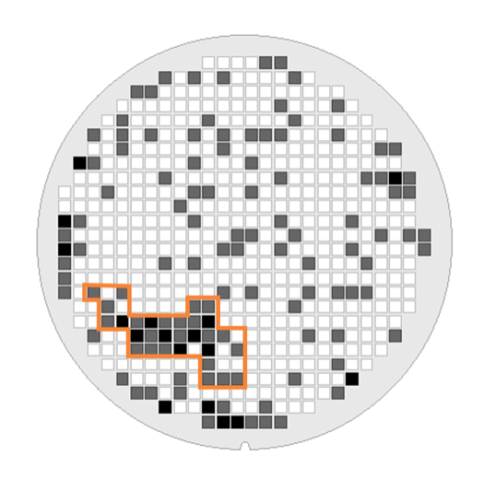
Fig. 4: Electrical test spatial outlier detection methods show macro-defects as localized clusters. Source: PDF Solutions
Major ATE companies typically have wafer test map data available after test. Efforts to perform detection in real-time on the test cell is an ongoing challenge.
“In general, we’re moving forward with AI/ML applications in testing, design, and manufacturing,” said Jin Yu, head of machine learning at Teradyne. “Our work on defective wafer image detection is a collaboration with a customer. There have been multiple papers that investigated various algorithms. In a recent paper [1], the authors identified eight classes of wafer test map images using a Kaggle data set [2,3]. What we did is a little bit different. First, we did our own labeling and classified it into four types — centered, local clusters, random, and scrap. Scrap is relevant to some macro-defects. It depends on how big the scrap image is. It might be a macro problem. It might be a micro problem. Second, the algorithm we used in our own development differs from the traditional computer vision-based approach.”
Yu noted that Teradyne’s approach used Meta DinoV2 [4,5] (a vision transformation approach [6]) as an image foundation model trained upon millions of images to get the image embeddings as their signatures. To train for defective wafer detection they used circle images instead of wafer test maps. The results from the Meta DinoV2 feed into a light gradient boosting machine (LGBM) [7] algorithm that performs a decision-tree analysis to classify the wafer test maps into the four classes. He noted that combining these two algorithms outperformed traditional computer vision-based approaches. With customer wafer test data, 98% accuracy was achieved versus 95% accuracy for either neural network- or vision transformer-based approaches alone.

Fig. 5: Real-time wafer defect categorization using advanced machine learning algorithms. Source: Teradyne
Conclusion
Inspection for macro defects occurs throughout wafer manufacturing, starting with silicon ingot cuts. But because of the wide variation in the causes of macro defects, a variety of inspection methods are needed, including optical, infrared, and X-ray diffraction. And the earlier this is done, the less scrap.
That’s not always possible due to a multitude of reasons, so engineering teams continue to use wafer test map analysis to identify macro-defects. From there, traceable data can be used to improve the upstream process or modify the inspection strategy.
“The emergence of new technologies such as compound semiconductors, chiplets, wafer-level assembly, and more introduce new needs for macro-inspection,” said PDF’s Zamek. “This is happening across the entire manufacturing flow, from crystal growth through fab inline steps, back-end and assembly and test. That’s where many of our customers see the benefit of deploying enterprise-wide analytics, breaking the data silos.”
References
Related Reading
X-ray Inspection Becoming Essential In Advanced Packaging
Improvements in speed and precision have transformed a research tool for studying defects in chips into an industry workhorse.
Better Inspection, Higher Yield
Weighing the tradeoffs of macro- and micro-inspection, and a combination of both.
Inspecting, Testing, And Measuring SiC
Demand for solutions is booming, but the technology is just beginning to gain its footing.
Fabs Drive Deeper Into Machine Learning
Wafer image interpretation can impact yield and throughput.
 |
 |
 |
 |
 |
 |
 |
Leave a Reply