EUV progress report; 3D metrology; giant microscopes; DSA mania.

EUV progress report
At the SPIE Advanced Lithography conference in San Jose, Calif., ASML Holding said that one customer, Taiwan Semiconductor Manufacturing Co. Ltd. (TSMC), has exposed more than 1,000 wafers on an NXE:3300B EUV system in a single day.
This is one step towards the insertion of EUV lithography in volume production. During a recent test run on the system, TSMC exposed 1,022 wafers in 24 hours with sustained power of over 90 Watts.
“This compares to just 10 Watt at the same conference last year. (TSMC) noted that this has been a struggle, but that the roadmap to 125 Watt by Q2/Q3 this year looks achievable. So far, the new source design from ASML seems to be working well, which is a positive for ASML. Still, the power is short of the 250 Watt that is needed for high-volume manufacturing (HVM), so there is much work ahead,” said Weston Twigg, an analyst with Pacific Crest Securities, in a report.
Indeed, EUV has made progress, but there still are issues with the power source, resists and masks.
“TSMC demonstrated good overlay results, but noted that other areas like resist need further improvement. Mask defects appear manageable for now, but improvement is needed for HVM, and ultimately TSMC agrees that an actinic mask inspection tool is needed. We look for a possible joint investment in KLA-Tencor’s EUV mask inspection program later this year,” Twigg said.
In any case, 193nm immersion and multiple patterning could push out the need for EUV. “Yan Borodovsky from Intel presented an interesting paper on using pitch splitting (multiple patterning) to extend Moore’s Law to at least 5nm. He argued that with aggressive area scaling, Intel can offset the increasing cost of lithography,” Twigg added.
3D metrology
At SPIE, Applied Materials rolled out an in-line CD SEM metrology tool. The tool, dubbed the VeritySEM 5i, is designed for use in measuring high-aspect ratio and complex features of 3D NAND and finFETs.
The tool solves a major problem. The industry is moving from planar to 3D-like devices, such as 3D NAND and finFETs. But yet, 2D metrology is struggling to measure these 3D-like devices.As a result, there is a pressing need for a new metrology tool that supports 3D measurements, according to Ofer Adan, global product and technology manager at Applied Materials.
The new tool from Applied has resolutions down to 1.2nm with image enhancement. The previous tool from the company had 1.45nm resolutions.
The new tool features a high-resolution SEM column, tilted-beam, and backscattered electron (BSE) imaging. The tilt-beam provides in-line measurements for finFET sidewalls, as well as gate and fin height. BSE imaging for via-in-trench bottom CD enables chipmakers to ensure connectivity between underlying and overlaying metal layers. And it enables measuring the asymmetrical sidewall and bottom CDs of 3D NAND devices with high aspect ratios reaching up to 60:1 and beyond.
Giant microscopes
A new and giant electron microscope that can pinpoint the position of single atoms has been unveiled by the Engineering and Physical Sciences Research Council (EPSRC).
The £3.7 million Nion Hermes Scanning Transmission Electron Microscope, one of only three in the world, is situated at the EPSRC SuperSTEM facility at the Daresbury lab complex near Warrington, U.K. EPSRC is the main U.K. government agency for funding research and training in engineering and the physical sciences.
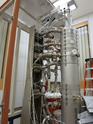
Super scope: The Nion UltraSTEM 100 MC HERMES (Source: EPSRC).
The microscope boasts the world’s highest energy resolution at 10meV. The system also has a high spatial resolution, operating in this energy range of 0.1nm at 60kV and 0.8nm at 100kV.
It also consists of flexible post-specimen optics, which enables large EELS collection angles and a flexible imaging detector setup. It also includes an UHV Gatan Enfinium spectrometer, including fast shutter and dual EELS capabilities.
DSA mania
On Oct. 26-27, 2015, Imec will organize, in collaboration with Sematech, EIDEC and CEA-Leti, the 1st International Symposium on directed self-assembly (DSA). The aim of the symposium is to identify key remaining challenges for insertion of DSA into semiconductor manufacturing and to identify potential solutions.
Meanwhile, at this week’s SPIE, Imec and its partners will present its progress on DSA on three fronts. First, Imec, TEL and Merck have improved DSA defectivity in the past year, approaching single-digit values. Imec and its partners achieved defectivity values of 24 defects/cm2.
Reducing defectivity is one of the main roadblocks in DSA. “Over the past few years, we have realized a reduction of DSA defectivity by a factor 10 every six months,” stated An Steegen, senior vice president of process technologies at Imec, on the organization’s Web site. “Our processes show the potential to achieve single-digit defectivity values in the near future without any technical roadblocks lying ahead.”
Second, the partners have developed a DSA solution for a via patterning process at 7nm. This required a novel template DSA process by using a polystyrene (PS)-wetting scheme. This process reduces the critical dimension (CD) of the template. And it has more advantages than the conventional polymethylmetacrylate (PMMA)-wetting scheme. In addition, an etch process has been developed to transfer the small vias (~15nm CD) into the underlying hard mask.
And third, Imec has developed a new chemo-epitaxy flow for 30nm and 45nm pitch hexagonal holes patterning using a single 193nm immersion exposure. The technology could be used for DRAM applications.

Imec’s chemo-epitaxy flow for DSA (Source: Imec)
 |
|
 |
|
 |
 |
 | |
 |
 |
Leave a Reply