The IC industry is struggling with blurring lines between different disciplines as chips are more tightly integrated with software in packages and systems.

Complexity in hardware design is spilling over to other disciplines, including software, manufacturing, and new materials, creating issues for how to model more data at multiple abstraction levels.
Challenges are growing around which abstraction level to use for a particular stage of the design, when to use it, and which data to include. Those decisions are becoming more difficult at each new node, as more devices are integrated into larger systems, and as more steps in the design flow shift both left and right.
“In electronic design, SPICE is the simulation environment best suited to transistor-level design, perhaps extending to the complexity of a basic logic building block,” said Simon Davidmann, CEO of Imperas Software. “But for SoC design, with possibly billions of transistors, different jumps in abstraction are required. For example, there is the gate-level boundary that forms the basis of the RTL design of the more complex structures of processors and beyond.”
Creating an executable instruction set model that works for both the hardware and software teams is critical for a design to hit a market window. By using a golden reference model with a step-and-compare methodology, verification can be done at the instruction boundary and configured in a UVM SystemVerilog testbench for asynchronous events and debug. But this also is becoming harder to achieve.
“It becomes the dynamic reference, and can become the heart of a simulation of the whole system as a virtual platform or virtual prototype,” Davidmann said. “As multicore designs become mainstream, with hundreds or thousands of cores, the same challenge can be seen in finding the ideal balance in abstraction in accuracy over capacity. It is the key requirement for simulation. But what level of modeling provides the most useful reference for designers? With simulation technology, it is possible to simulate the complete design with instruction-accurate models for a programmer’s view of the total system. In the case of AI or ML applications that have been developed in cloud-based environments, a large amount of analysis and tuning has already been completed. Today, hardware/software co-design is becoming more of a software-driven analysis of hardware structures, with complete simulation of large data sets and real-world situations.”
Partitioning of the design can help, breaking it into more manageable parts. The key is knowing what to split and when. “Configuring an array of processors as an AI/ML hardware accelerator can be split between the top-level design and the key subsystems,” he said. “Often the key algorithms will be partitioned to a processing element with, for example, two to five CPU cores plus hardware engines, such as RISC-V Vector Extensions or Arm SVE2. In turn, this processing element will be replicated in the design tens to thousands of times. A virtual platform provides the abstraction necessary for first level of tradeoff analysis and development. This leads to a verification reference model for the individual RISC-V cores, as well as a complete model of the SoC for software development. As in the case of the gate-level boundary in previous abstractions, the instruction-accurate boundary unites the hardware and software teams, and is the natural basis for the next levels of abstractions in this post-Moore’s Law era of heterogeneous multicore compute platforms for AI and ML.”
This isn’t just confined to a single chip. Consider the design of 5G wireless systems for connecting automotive, radar and semiconductor technologies. Those systems are constantly being pushed to operate at higher frequencies, resulting in a corresponding increasing in packaging density for different components and more sophisticated packaging requirements.
“More and more, designers must focus on the physics, namely the electromagnetic (EM) effects caused by greater coupling between the various parts of the circuit, as well as the thermal issues resulting from component density,” said Sherry Hess, product marketing group director for system analysis and signoff at Cadence.
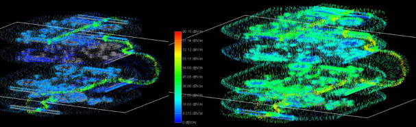
Fig 01: 3D modeling of a rigid-flex PCB. Electromagnetic analysis of rigid-flex PCBs has historically been challenging due to the complexity of 3D designs. Source: Cadence
Electrical performance of these systems often degrades as speeds increase and layouts become denser, making EM simulation critical for enabling designers to model and control the signal, power and thermal integrity issues within the system. “As the various components in the system interact with each other, the size of the problem increases, and the simulator must be able to keep pace and handle larger and more complex designs,” Hess said. “This has led to an emphasis on parallel job distribution and interest in cloud-based computing most recently.”
This means the EM simulator must be capable of handling large systems involving multiple technologies, such as flip-chip on interposer. Thermal simulation is also critical for these systems. The increased speed and density of the components requires that the extra heat generated by the active circuitry be efficiently dissipated through the system, posing a challenge for the package designer, for instance.

Fig. 02: Thermal analysis is more complex with interconnected electrical and thermal effects. Source: Cadence
“As the need to model the physical issues like EM coupling and heat dissipation grow, electronic design automation (EDA) software must meet the challenges presented by the need for improved simulators,” Hess said. “A user-friendly design environment is also required that offers an efficient front-to-back end interoperable workflow. This enables designers to efficiently switch between various simulation tools and environments, and to share results with other teams in order to achieve high-performing electronic systems that win in the end market.”
Overlapping challenges
Still, there are more pieces to put together, and optimizing everything so it works well, and throughout its expected lifetime, remains a challenge.
“With smaller geometries, DRC can be done on local level, e.g., the transistor or standard cell level,” said Andy Heinig, department head for efficient electronics at Fraunhofer IIS’ Engineering of Adaptive Systems Division. “In this case, it needs more verification time but it can be handled the classical way — with extensions of the DRC rules in the tools. But in the newest nodes, the power/ground problem is a global problem.”
With each new node, the supply voltage is decreased. That, in turn, reduces the headroom for voltage drops. The power consumption on place A can imply that the voltage delivery on a place B is in a different position then place A, he said. “This means it is a global effect that needs a lot of consideration in the newest nodes. It also needs more support in the design tools, starting from the analysis of the used power per standard cell or area up to the simulation of the whole power grid with extracted parasitics.”
Atomic-scale modeling
Shrinking features and more complexity are eroding the line between design and manufacturing, as well. As a result, design teams now need to consider the impact of different materials and structures, effectively pushing them into the same kinds of atomic-level modeling that foundries and materials scientists have been wrestling with for the better part of a decade.
“Approximately five to seven years ago, when many of the semiconductor companies starting to look more closely at materials and began doing materials innovation and materials engineering, we started thinking about what was needed to shift left to pathfinding,” said Terry Ma, vice president of R&D at Synopsys. “We rely on some silicon data to calibrate our models, but when you’re exploring new materials and new devices, there’s no silicon data.”
This is where atomic-scale modeling comes into play. It can be used to generate a material’s properties and the characteristics that can feed into TCAD so the engineering teams can either develop new models or calibrate existing models for new materials.
“The idea is that we went from atomic scale to the device level and then the cell level,” Ma said. “TCAD typically is a couple of transistors’ characteristics, but when we expand into what we call DTCO (design technology co-optimization), we no longer just can rely on a single transistor. We started with SRAM cells, then to flip flops, and to I/O, in trying to understand the cell level of characteristics in order to see the impact on technology, on design, and vice versa. Now we’re going to the block level, meaning that we can connect to place-and-route, to many-library design, etc. Atomic-scale modeling is key to help engineering teams explore new options and new materials.”
Scaling adds some unusual hurdles, as well. “We’re scaling all dimensions,” observed Ronald Gull, director of TCAD at Synopsys. “We’re scaling layered thicknesses. So all of a sudden a lot of material parameters change. A crystalline bulk cell has its own properties, and you can plug them in all the way up to the block level or the SPICE level. But then you make it so small that the interactions of the layers change the material behavior. So scaling actually changes material properties and we need to capture that.”
It also creates a need for different materials. “We need higher k dielectrics, lower k dielectrics in the interconnect, and we need to understand why very thin wires start to have high resistance. There’s a lot of effort going into the gate scaling, gaining the physical understanding and then feeding that back to the whole process. That’s one very important aspect of atomic-scale modeling, on top of just being able to actually push the R&D of the next level device.”
Material properties impact both logic and memory. “We started addressing this in logic, but the memory industry also has started to look at emerging issues and new materials coming into play,” Ma said. “There are new challenges even for power applications. With wide-bandgap materials, the behavior is slightly different than silicon. For power, especially when you want to go to very high voltage, there are thousands of volts with silicon carbide and gallium nitride. On top of that, now people are looking at gallium oxide as another new material. And these are not exactly single materials. They’re compound materials that allow you to look at even higher voltages for power. So the materials modeling in the semiconductor industry is not only for logic or memory, but also for power.”
Traditionally, the TCAD group would get involved later in the design process. This is changing, which in turn is having an impact on which teams interact with the data and when that happens.
“When we talk to IDMs or foundries, they have DTCO — which used to be called DFM, and is now also referred to as silicon enablement,” Ma said. “Those teams are responsible for looking at, ‘If I use this technology, how will the design fit into this technology?’ The manufacturers need to make sure the technology can work for multiple designs. By exploring early on, they can see if changes need to be made to adjust for the threshold, for example, and what they need to do for specific customers. When a design comes in, they want to make sure the design works — not when it is in production, but during the pilot and the risk production run, etc.”
Another challenge that crops up with scaling is edge placement error, which used to be something design teams rarely worried about. But as tolerances tighten and margin shrinks, these kinds of issues have pushed much further left, and the tools are being extended further right. In addition, the models being developed need to be more accurate because of those tighter tolerances.
“Something that may have been acceptable two nodes ago is no longer acceptable, and your models have to keep up with that ever progressing specification,” said Germain Fenger, senior product manager, Calibre product management group at Siemens EDA. “Specifically in the lithography process, every few nodes we have had to focus a lot on the resist process, which is probably the biggest component in the lithography process in terms of modeling. And then when there are new advances in the actual lithography tools, we need to incorporate those changes to the lithography system. The move to EUV, and the subsequent move to high-NA EUV, both are significant departures from our traditional optical lithography modeling. There are new effects that we need to account for in those models that weren’t as important in older lithography systems.”
Fenger pointed to two important drivers at the 2nm node — etch modeling and curvilinear optical proximity correction. “After the lithography process is done, we then transfer that into an underlying film, and that has its own proximity effects that we need to account for. The other new challenge at 2nm is curvilinear OPC. When you move to curvilinear OPC, this is a significant departure from modeling Manhattan shapes. Now we have to model all angled shapes, so we had rethink our 3D mask model that we use in the lithography simulator to handle these new all angled shapes. There are two aspects to this. One is the accuracy. The other is the runtime. When you include all angled shapes, you’re essentially increasing the edge count of a given post OPC design by an order of magnitude, because where something was defined by four edges it’s now maybe defined by 100 or more. The things that used to be fast, and that we didn’t care about, we now have to rethink because they’re far too slow. So a lot of effort is going into both the accuracy and the runtime aspects of curvilinear masks.”

Fig. 1: Etch modeling challenges at each new node. Source: Siemens EDA
Conclusion
Traditional lines of demarcation in design are blurring, making it increasingly difficult to balance a variety of factors and optimize designs.
Synopsys’ Ma said the first challenge is to make sure the physics are correct. “This is about true connectivity, allowing multiscale simulation and fast turnaround time so you don’t have to wait for three months to find out whether it will work or not, and instead find out in a week or maybe two. As part of this, we are embracing machine learning capabilities to keep pushing the limit for physics. You need to be sure you’re not sacrificing a lot of accuracy just to get to a larger scale.”
In effect, everything has to work together in very tight spaces. “You bring in more individual atoms, you see how they influence the whole behavior,” said Gull. “Then that needs to be abstracted to the device level, to the cell level. Increasingly, you need to keep these links from one level to the next so that you can actually make predictions that are valid on the system level. That’s a hard thing to do.”
When it comes to making multiscale simulation run faster, it’s not just about giving parameters to the physical model. “Now if you go to a completely new material, like gallium oxide, these models are too slow to develop,” he said. “So we need to find ways where we abstract the model from atomic scale, we go to a physical informed machine learning model that can do the same. It keeps the physics, but it’s much faster. Then we try to scale that, and accelerate the multiscale build up so that we still have enough valid physics before developing a full new model on one of these levels.”
To make matters more complicated, models need to scale from the atomic to the system level, and they need to work across the design flow, which includes both hardware and software, and even into manufacturing. “That is a hard problem, but that’s what the users want today,” Gull said. “When they need to make a decision about whether to add ruthenium into their flow, they need to understand what it means to the PPA capacitance in the end, and whether the cost of bringing in ruthenium outweighs the performance gained. And they’re doing this exercise from forming the metal in this tiny space all the way up to what does it mean on the system level. These are the questions that SoC engineering teams need to ask when they try to make decisions about dramatic changes, such as changing an element in the back end.”

 |
|
 |
 |
 |
 |
Excellent article thanks. I would be happy to know
minimum iin EDA features on many nodes say 28 nm to 3 nm. Just what I see on bottom layout. Is it less than 1 nm ?
?. Can one use that as a minimum even if lines and parts of transistors are larger. Is there any mathematics in EDA to operate on calculated vdimensions smaller than on real chip.