Efficient heat dissipation is critical in fan-out packages.

As chip performance and integration continue to advance, thermal dissipation control has become increasingly critical not only at the wafer fabrication level but also in the packaging industry. For artificial intelligence (AI) and high performance computing (HPC) applications, the industry is gradually shifting toward 2.5D integration. In response to the growing demand, High-Density Fan-Out (HDFO) packaging has emerged as a key solution. Consequently, the need to enhance the thermal dissipation performance of fan-out packages has also increased.
In particular, the S-SWIFT package is designed to accommodate high-performance chips with increased integration density. This trend has led to larger body sizes and higher copper (Cu) densities. To ensure reliability, molded structures are also being adopted at the same time, and these characteristics make efficient heat dissipation a critical requirement. To address this, metal lids combined with thermal interface materials (TIMs) are commonly employed. Among various TIM options, including solder TIMs (sTIMs) based on indium or indium alloys, are considered promising due to their excellent thermal conductivity. However, sTIMs cannot be used alone, they require backside metallization (BSM) on the module to establish a thermal path and adhesion between the lid, sTIM, and the module.
Conventional BSM processing has evolved for power devices and typically involves high-temperature steps, which are unsuitable for S-SWIFT modules. Moreover, the requirements for BSM in power devices differ from those in S-SWIFT, so consideration of different fabrication methods or stack-ups for S-SWIFT is occurring. Epoxy molding compounds (EMCs) used in fan-out packages generally have a glass transition temperature (Tg) in the range of 150–190°C, and exposure to temperatures above Tg can induce tensile stress and increase the risk of deformation. Additionally, depending on the bump composition, post-chip-attach processes that expose the package to temperatures exceeding 230°C can accelerate intermetallic compound (IMC) growth at the bump joints, leading to increased brittleness and reduced package reliability.
This study proposes alternatives to conventional BSM structures by considering the process and performance requirements derived from the structural characteristics of fan-out packages. The proposed approach is based on a low-temperature manufacturing process, and its performance is evaluated in terms of solder TIM coverage. Furthermore, the advantages and limitations of potential BSM process flows applicable to the S-SWIFT package are reviewed and the findings of the implementation sequence of BSM in the S-SWIFT process are summarized.
In the wafer fabrication industry, aluminum (Al) is typically used as the bottom-most layer in the BSM structure to form ohmic contact between the silicon (Si) substrate and the lead frame. This is achieved either by depositing BSM at temperatures above 300°C or by annealing post BSM deposition to induce “spiking,” which refers to Al interdiffusion into the Si substrate. However, such a high-temperature process significantly exceeds the Tg of the EMC, rendering them unsuitable for fan-out packages with molded structures. As described in Fig. 1(b), the S-SWIFT structure does not require an electrical path from the Si die to the metal lid, thereby eliminating the need for Al spiking. Consequently, low-temperature BSM fabrication processes can be applied to fan-out packages and S-SWIFT modules.

Fig. 1: Structure and current flow of power device and S-SWIFT packaging. (a) Power devices – vertical connection of thermal and electrical (illustrated only soldering area between die and Cu with BSM) and (b) S-SWIFT design- vertical connection of thermal but no electrical connection.
This study investigated whether differences in BSM stack-up and a low-temperature fabrication process affect the degradation of sTIM coverage after reliability testing. The results indicate there is no significant difference in sTIM coverage or adhesion performance, even when the BSM is fabricated using a low-temperature process without an Al layer. This suggests that low-temperature BSM processes are viable for fan-out package applications.
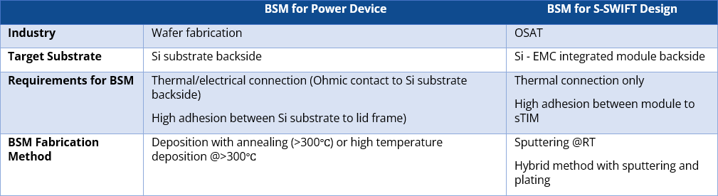
Table 1: Comparison of BSM requirements between wafer fabrication and OSAT.
To enable compatibility with molded structures, the BSM process was designed to operate below 200°C. A hybrid process combining sputtering and plating was examined, evaluating both the process conditions and resulting performance. For BSM fabrication using sputtering, a simplified stack-up of titanium/nickel-vanadium/gold (Ti/NiV/Au)—excluding aluminum—was evaluated as the baseline for the S-SWIFT design which does not need an electrical connection between the Si die and the metal lid.
Sputtering for both sputtered and plated BSM was conducted at room temperature (RT), the overall maximum temperature (Tmax) during the process, including the degassing step prior to RF etching and deposition on the molded wafer, was measured to be 180°C based on thermo-label indicators.

Fig. 2: Stack-ups of BSM. (a) conventional stack-up for power device, (b) stack-up for S-SWIFT design, (c) stack-up of hybrid process of sputtering & plating.

Table 2: BSM stack-ups and fabrication methods for S-SWIFT design.
All evaluations were conducted using a chiplet-based large-body S-SWIFT module with a minimum module size of 26.7 mm, incorporating a multilayer redistribution layer (RDL) package design. To assess the reliability of sTIM coverage, the samples were subjected to Unbiased Highly Accelerated Stress Test (uHAST), High Temperature Storage (HTS), and Temperature Cycling under Condition G (TCG). The performance was evaluated based on sTIM coverage, which was determined using Through-transmission Scanning Acoustic Microscopy (T-SAM) imaging.

Table 3: Reliability test conditions.
Depending on the devices and the purposes of BSM, various stack-up configurations can be implemented. In particular, when electrical functionality is not required, the Al layer may be not applied or replaced with alternative materials.
A typical BSM stack-up consists of Al (adhesion layer), Ti (barrier layer), NiV (soldering layer), and Au (protection layer). Among these, Al serves not only as an adhesion layer but also facilitates ohmic contact formation with the device by promoting interdiffusion into the Si substrate through annealing post deposition. As previously discussed, this interdiffusion—commonly referred to as “spiking”—requires deposition or annealing temperatures of at least 300°C.
However, in fan-out packaging, post-deposition annealing over a Tg of EMC is avoided to prevent thermal degradation of EMC and solder joint reliability. Without annealing or deposition over 300℃, Al cannot diffuse into the Si substrate. However, if sufficient mechanical adhesion between the module and BSM can be achieved without Al, the layer may be excluded or substituted, thereby enabling the use of low-temperature BSM processes.

Table 4: Test vehicle information for comparison of sputtered BSM.
To evaluate the impact of the Al layer on sTIM reliability in low-temperature BSM processes, the test vehicle (TV) design described in Table 4 was applied. Reliability tests were conducted using uHAST, HTS, and TCG. No significant differences were observed between BSM structures with and without the Al layer.
Table 5 shows sTIM coverage by TCG. The sTIM coverage remained above 99% for both configurations up to TCG 600 cycles, regardless of the presence of Al. A slight degradation of less than 3% was observed beyond 600 cycles, with coverage still exceeding 96% at 1000 cycles as described in Fig 3. These results indicate that the absence of an Al layer in low-temperature BSM process does not adversely affect sTIM coverage or reliability.

Table 5: T-SCAN images of modules with sputter BSM – Al/Ti/NiV/Au & Ti/NiV/Au after Temperature Cycles under condition G (-40 to 125℃).

Fig. 3: sTIM coverage of sputtered BSM – Al/Ti/NiV/Au & Ti/NiV/Au by TCG. Observed average 2.10% and 2.26% of coverage degradation on Al/Ti/NiV/Au and Ti/NiV/Au after TCG 1000X.
Under HTS up to 1000 hrs and uHAST up to 264 hours conditions, the sTIM coverage remained above 99.7% as shown in Table 6 and 7, demonstrating reliable performance. These results suggest that, exposure to thermal cycling provides a more meaningful indication of degradation levels than static thermal stress when evaluating the reliability of sTIM coverage. TCG tests revealed more pronounced changes in coverage, highlighting their importance in assessing long-term reliability.

Table 6: T-SCAN images of modules with sputtered BSM – Al/Ti/NiV/Au & Ti/NiV/Au by HTS.

Table 7: T-SCAN images of modules with sputtered BSM – Al/Ti/NiV/Au & Ti/NiV/Au by uHAST.
To explore an alternative to deposited BSM, a plating-based BSM process using the test vehicle design described in Table 8 was evaluated. The reliability of the plated BSM was assessed by examining sTIM coverage in the packages.

Table 8: Test vehicle information for plated BSM.
When plated BSM was applied, degradation under uHAST up to 264 hours and HTS up to 1000 hours was negligible, similar to the results observed with sputtered BSM. Under TCG up to 1000 cycles, a maximum degradation of 2.40% in sTIM coverage was observed for the plated BSM. This level of degradation is comparable to that of the sputtered BSM. The variation in sTIM coverage across different BSM conditions under Temperature Cycling is described in Figure 4.

Fig. 4: sTIM coverage of all BSM conditions at EOL & TCG 1000X. All samples showed above 95% of sTIM coverage by TCG 100X and the degradation of sTIM coverage was less than 3%.
For the S-SWIFT package, the process flow follows the sequence of RDL interposer → chip attach → backside Cu pillar bumping → module attach. Depending on the implementation sequence of the BSM process based on this process flow, two distinct approaches can be defined. For this study, the process where BSM is applied prior to backside Cu pillar bumping is “BSM First,” and the process where BSM is applied after bumping is completed is “BSM Last.” Evaluations related to the sequence of BSM application were conducted based on the Al/Ti/NiV/Au stack-up configuration on the TV in Table 9.

Table 9: Test vehicle information for comparison of process flow.
From a process flow perspective, the key differences between the two approaches are as follows: the BSM First method offers a simpler process and allows the use of a single carrier, which is advantageous. In contrast, the BSM Last method requires BSM deposition on the backside of the Cu pillar bumps after the completion of bumping. To protect the Cu pillars during BSM deposition, an additional second carrier and wafer support system (WSS) process are necessary.

Fig. 5: The process flows for S-SWIFT design by BSM. (a) BSM First, (b) BSM Last.
Since BSM deposition in the BSM Last flow occurs at the end of the bumping process, WSS is not applied to the BSM surface, resulting in a relatively lower risk of surface contamination. As shown in the XPS analysis results in Fig. 6, the BSM Last condition exhibited lower levels of carbon and oxygen compared to the BSM First condition. Notably, trace amounts of fluorine (0.7–2.4 at.%) were detected in the BSM First samples, which is presumed to originate from polymeric residues introduced during WSS application on the BSM surface.
As shown in Fig. 7, plasma treatment restored the BSM surface cleanliness to a level comparable to that immediately after deposition. Furthermore, as illustrated in Fig. 8, sTIM coverage under TCG conditions remained consistent regardless of the BSM application sequence. These results suggest that, in the BSM First flow, plasma treatment applied prior to sTIM attach can effectively enhance wettability while simultaneously recovering BSM surface cleanliness.

Fig. 6: XPS analysis results by process flow.

Fig. 7: XPS analysis result by downstream process on BSM First.

Fig. 8: The sTIM coverage of BSM First & BSM Last by TCG. Observed degradation of sTIM coverage is less than 1%.
A comparison of wafer and module warpage based on the sequence of BSM application revealed that, after module singulation and module & lid attach, no significant difference in warpage was observed at the package level.
Based on these findings, the sTIM reliability performance between the BSM First and BSM Last process flows were found to be comparable. Both BSM First and BSM Last process flows are considered viable options for implementation in the S-SWIFT fan-out packaging platform, depending on the specific design and reliability requirements.

Fig. 9: S-SWIFT package warpage trend by BSM process flow.
This study investigated the impact of various BSM fabrication processes and stack-up configurations on package reliability in fan-out packages, specifically those employing the S-SWIFT module, from the perspective of sTIM coverage. Reliability assessments were conducted under HTS, uHAST, and TCG conditions, focusing on the presence or absence of Al in the BSM stack and its associated processing methods.
The results demonstrate that in S-SWIFT packages where Ohmic contact between the BSM and the device is not required, low-temperature BSM fabrication is feasible and beneficial in terms of sTIM coverage. Furthermore, the findings suggest that alternative adhesion materials can be employed in place of Al, enabling low-temperature processing while maintaining adequate adhesion and reliability. These insights provide a viable pathway for optimizing BSM integration in fan-out packaging technologies.
To learn more about Amkor’s S-SWIFT technology, visit https://amkor.com/technology/s-swift/.
 |
|
 |
|
 |
 |
 | |
 |
 |
Leave a Reply