Derivative-free techniques for solving problems where gradient-based methods fall short.

As semiconductor technologies advance, device structures are becoming increasingly complex. New materials and architectures introduce intricate physical effects requiring accurate modeling to ensure reliable circuit simulation and design. Correspondingly, these accuracy requirements raise demands on the accuracy and efficiency of device modeling.
Modern device models often involve hundreds of interdependent parameters. Effects like short-channel behavior, mobility degradation, and self-heating are highly correlated, creating a nonlinear parameter space that is difficult to optimize. Traditional optimizers, while useful for local tuning, often get trapped in local minima during global optimization, resulting in lengthy, manual, and error-prone modeling flows.
To overcome these limitations, this blog explores how Machine Learning (ML) is revolutionizing the model extraction process. ML-based optimization efficiently navigates complex, multivariate parameter spaces, achieving better convergence and higher accuracy, with significantly less manual tuning and designer effort. Using ML opens the door to more automated, robust, and scalable modeling flows that keep pace with today’s rapidly advancing semiconductor technologies.
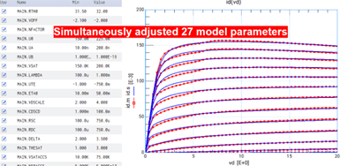
Compact models rely on numerous parameters to simulate device behavior under various conditions. For simple devices, such as a Schottky diode, this might involve just three parameters. But for modern devices like GaN HEMTs or advanced CMOS transistors, the number of parameters can easily exceed hundreds.
Traditional gradient-based optimization algorithms—such as Newton-Raphson or Levenberg-Marquardt—struggle in this environment. These methods often:
As a result, engineers often spend days or even weeks fine-tuning models, with no guarantee of finding the global optimum.
To address these limitations, Keysight is shifting toward gradient-free optimization algorithms. These methods are more robust against noise, better suited for non-convex landscapes, and less dependent on initial conditions.
At Keysight, we’ve developed the ML Optimizer, a machine learning-based solution designed specifically for compact model parameter extraction. It combines the strengths of gradient-free methods with adaptive learning to deliver:
The ML Optimizer continuously learns from each iteration, refining its strategy to balance exploration and exploitation. It’s particularly effective for automated extraction applications, where stability and accuracy are critical.
Both the Genetic Optimizer in IC‑CAP and the ML Optimizer are powerful derivative-free techniques for solving problems where gradient-based methods fall short. The ML Optimizer, designed for continuous optimization, generally outperforms the Genetic Optimizer in speed and precision on convex problems. It automatically adapts step size and search direction, balances exploration and exploitation with minimal tuning, and achieves faster convergence in high-dimensional spaces.
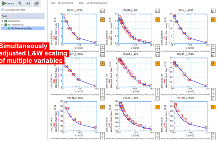
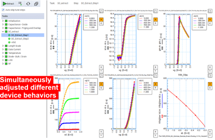
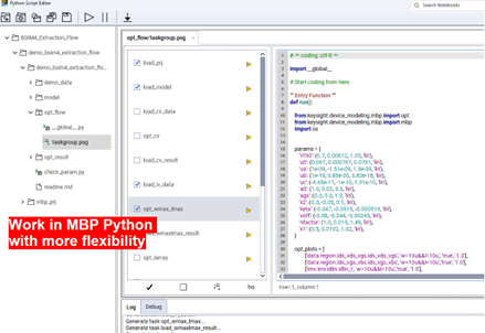
We’ve applied the ML Optimizer to a variety of device modeling scenarios:
Both Device Modeling IC-CAP 2025 and MBP 2026 integrate the new ML Optimizer, dramatically simplifying the workflow, reducing human error, and accelerating time-to-model, enabling a faster, more reliable path to high-quality results.
Adding ML represents a significant leap forward in device modeling. By leveraging machine learning, the ML Optimizer offers:
As semiconductor technologies continue to evolve, tools like the ML Optimizer will be essential for keeping pace with design demands.
For more details, check out the demo videos and application notes provided by Keysight.
 |
|
 |
 |
 |
 |
Really nice article! Thank you