Finding and fixing intermittent process excursions earlier.

Full-blown process excursions that affect every wafer are comparatively easy for fabs to detect and fix. However, “onesie-twosie,” lower-volume excursions can go unresolved for months or even years. Some process engineers call them “slow moving excursions.” And over time, those low-volume defects can add up to significant yield losses.
Some intermittent process excursions are ignored because they do not seem important enough to spend time on, like a faucet that occasionally drips. But more often, it is because the fab simply does not have enough data to investigate them. That’s because, for time and economic reasons, most fabs do not perform comprehensive in-line wafer inspection, and consequently, they have to rely much more heavily on end-of-line inspections.
In-line, a fab may only do partial-wafer sample inspection on a few wafers from a lot, and only at selected process steps. Unfortunately, such a low level of in-line sampling simply does not see a huge percentage of wafer real estate in the overall process, so it misses most of the intermittent process problems that occur. And if caught earlier, many of those intermittent problems could have been corrected earlier, to increase profitability.
The advent of next-generation macro defect inspection systems has now changed everything. These new tools are fast enough and economical enough to do macro inspection on 100% of the wafers in every lot at many more process steps.
It has been demonstrated that applying 100% macro defect inspection inline to all wafers in the lot and at many critical process levels enables a fab to catch many more low-level defects. And catching them sooner enables fabs to do more rework and minimize scrapped wafers. It also allows fabs to diagnose problem causes much more accurately, to realize net yield and profit benefits.
Here are two actual examples of the benefits of 100% inline macro defect inspection…
In this example, in-line macro inspection spotted an infrequently repeating defect that resembled a scratch (see Figure 1).
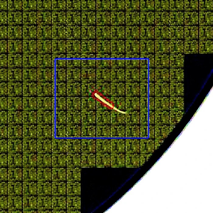
Fig. 1: Macro inspection detected this image.
This led to microscopic inspection, which revealed that the defect was actually an EBR drip (see Figure 2).
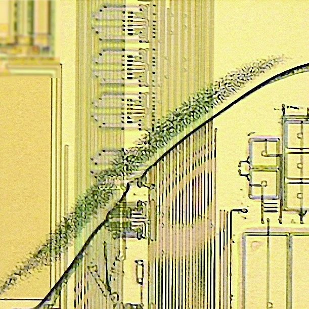
Fig. 2: Microscopic view revealed an EBR drip.
However, the problem frequency was low (see Table 1).
| Table 1: Defect-Affected Percentages | ||
| Lot % | 24 of 175 lots | 13.7% |
| Wafer % | 24 of 3,792 wafers | 0.6% |
The macro-inspection data was used to generate a jeopardy list of affected lots; however, a commonality analysis showed that many different tools and levels could potentially be involved.
Fortunately, the macro inspection platform was also able to track the slot position of each wafer at each processing step (see Figure 3), and this provided the most important clue – revealing that the majority of affected wafers were in slot #18.
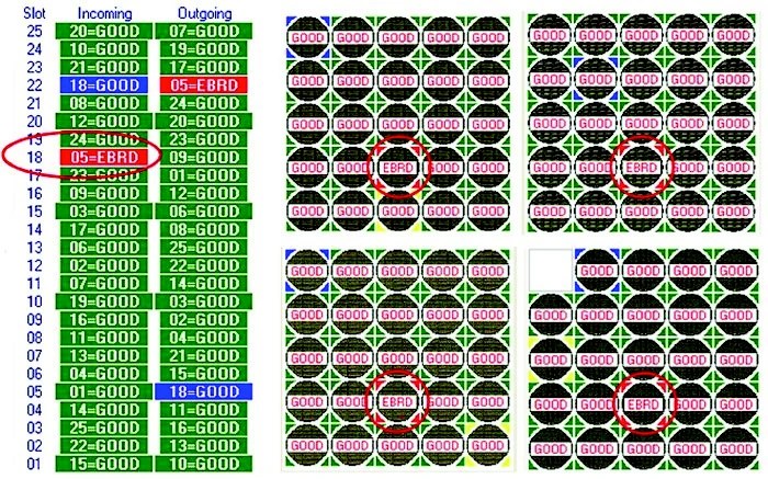
Fig. 3: Slot position analysis showed that the problem repeatedly affected the wafer in slot #18.
Upon further analysis, it was learned that an enhanced bowl wash had been recently implemented to clean the photoresist after each lot in an attempt to extend the time between cup changes.
Even after a lot had completed resist coating, wafers were still being processed in the workcell (expose and develop); and periodically one of the wafers on the robot arm would travel from slot #18 and pass by the “overspray” from the bowl wash – and a small droplet of PGMEA would fall on the wafer surface.
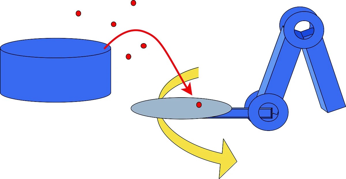
Fig. 4: Wafer on robot arm.
Without the abundance of data provided by 100% in-line wafer defect sampling it would have been extremely difficult to determine the root cause of this unique problem.
In this case, a defect was repeatedly being seen adjacent to the laser scribe (see Figure 4).
Initially, the problem was thought to be happening in the back end, and corrective actions were being considered there (adding dummy shots prior to CMP).
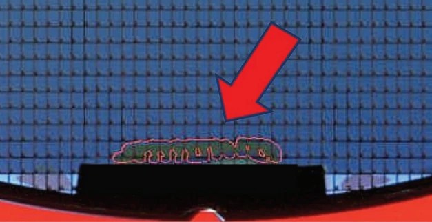
Fig. 5: Repeating defect seen near laser scribe.
However, a review of the in-line macro inspection images revealed that the defect was actually present much earlier in the process (see Figure 5), so the proposed back-end actions would not have corrected the problem.
The macro inspection tool specifically identified 1,249 wafers in 74 lots, and it was estimated that a total of between three and six thousand wafers were impacted, with a yield loss of 0.28% on each wafer.
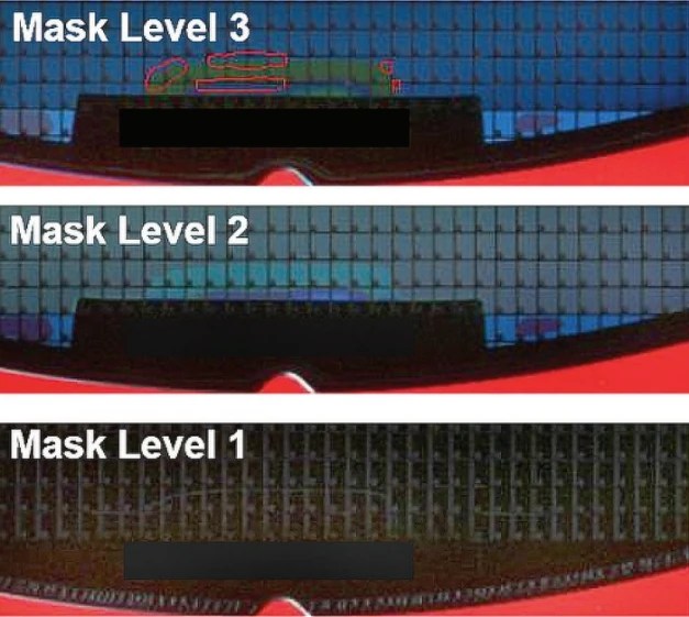
Fig. 6: Problem in the same area seen in earlier process steps.
Commonality analysis of the in-line inspection data was further able to pinpoint the source of the problem: a specific laser scribe tool with an incorrect scribe depth after a PM. The offending scriber was properly adjusted, and the problem ceased.
Once again, the comprehensive database built by 100% in-line macro defect inspection enabled the fab to zero in on the actual problem, which otherwise might have remained undiscovered much longer.
Identifying these types of low-level excursions early on – using the new generation of high-speed macro defect inspection systems like the EagleView from Microtronic – can be particularly helpful to fabs with yields above 80% or 90% who often find it difficult to achieve incremental improvements. Eliminating intermittent in-line defects that previously had been entirely missed can be an effective way to improve a high-performing fab’s numbers.
 |
|
 |
|
 |
 |
 | |
 |
 |
Leave a Reply