DFT should be integrated into tools throughout the development flow.

Back when semiconductor devices contained only a few thousand gates, manufacturing test was almost an afterthought. The development team threw the chip “over the wall” to the test engineers, who developed a set of test patterns for the manufacturing floor. As this process became more automated and chips became more complicated, test considerations crept into the development flow and design-for-test (DFT) techniques arose. Contemporary chips are so large and complex that a whole new set of challenges must be addressed.
In this age of pervasive intelligence, there are several key trends at work. One is silicon proliferation: with the Internet of Things (IoT), chips are everywhere. Many of these operate in difficult environments, putting pressure on the level of test required before parts are shipped. The intense computing demands of many applications, especially those based on AI, create huge power and thermal requirements that complicate test further. The era of software-defined systems means that virtually every chip is now an SoC, with processors used for self-test.
In addition, the wide use of pre-defined IP in complex architectures requires hierarchical test techniques. Many applications have high requirements for safety as well as reliability, availability, and serviceability (RAS), with associated high-coverage test needed. Test must occur not just during manufacturing, but also in the field, to prevent catastrophic failures. Finally, the increasing choice of multi-die devices, such as 3D-IC design, adds new levels of difficulty to test the individual dies, the interconnects, and the assembled packages.
The only way to address all these challenges is for test to permeate every aspect of the semiconductor development flow. This new paradigm, dubbed test hyperconvergence, goes well beyond test engineers advising designers how to make test easier or implementation tools automatically inserting DFT structures. Test tools and the other tools in the development flow must have synergies that enable more efficient chip development and better test methods. Examples include:
There are many benefits to this hyperconvergence. Early DFT provides a “shift left” in the test process as much as possible while minimizing the impact of DFT on power, performance, and area (PPA) metrics. Design overhead for DFT is reduced, test pattern coverage and quality and improved, and test time is kept under control. Post-silicon data enables informed decision-making and better yield. Finally, test in the field detects faults due to silicon aging or environmental factors so that corrective action can be taken before the system fails.
While the benefits of this approach are clear, creating enabling electronic design automation (EDA) tools and associated IP is a major undertaking. The full suite of tools must be integrated into a unified flow so that the required synergies can be built in. It is simply not possible for chip developers to attain the same results by cobbling together tools from multiple EDA vendors and IP from many sources. Fortunately, Synopsys provides a proven test solution that delivers all the benefits outlined above, as summarized in the diagram below.
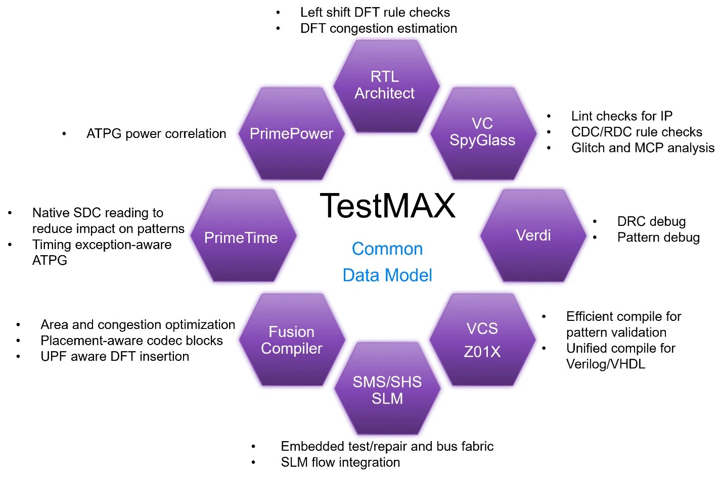
This solution is centered around the Synopsys TestMAX family of advanced test automation products. It starts at the architecture phase, with early testability checks and estimates of DFT impact. During RTL coding, Synopsys VC SpyGlass checks for violations of lint, clock domain crossing (CDC), reset domain crossing (RDC), glitch, and multi-cycle path (MCP) rules. Simulation supports efficient test pattern validation and fault grading in addition to functional verification. Issues found during simulation and design rule check (DRC) violations can be debugged easily.
The implementation flow, based on Synopsys Fusion Compiler, includes synthesis and layout of the design. Power-aware DFT insertion is performed at this stage, following the Unified Power Format (UPF) standard. ATPG is coupled closely with Synopsys PrimeTime static timing analysis using Synopsys Design Constraint (SDC) files for timing-aware pattern generation. Finally, the power impact of DFT and the power requirements for the patterns can be assessed. This flow uses the TestMAX common data model to ensure efficient and accurate communication.
The diagram above also shows examples of the test-related IP available. Synopsys Star Memory System (SMS) provides an end-to-end solution for embedded memory test and repair. It supports repairable and non-repairable memories across any foundry or process node, including such diverse types as eMRAM, TCAM, and eFlash. It connects to the Synopsys IP STAR Hierarchical System (SHS) to support other types of IP, including interface, digital, and analog/mixed-signal (AMS).
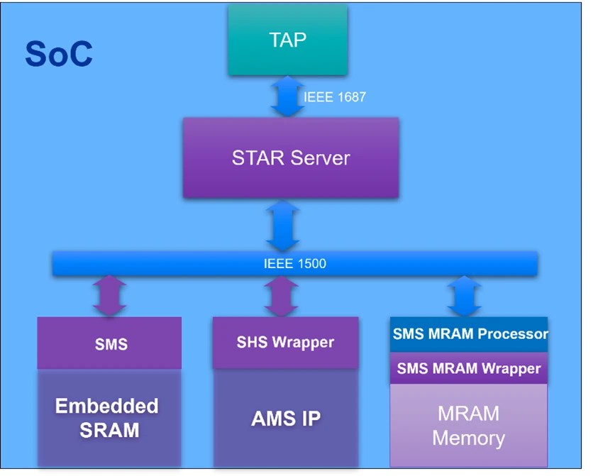
SMS supports advanced error correcting code (ECC) implementations with multi-bit detection and correction. This ensures data integrity and enhances RAS by correcting errors as they occur. This is required for safety-critical applications such as AI processors in self-driving cars. Synopsys also provides a portfolio of SLM IP such as process, voltage, and temperature (PVT) monitors and path margin monitors (PMMs) to perform in-field test and enable preventive maintenance.
In summary, it takes a broad and sophisticated test solution to support modern semiconductor devices. A few standalone test tools are no longer enough. DFT must be integrated into many tools in the development flow to provide true test hyperconvergence. This unified flow must be supported by appropriate IP for test and, when possible, repair during mission-mode operation. Choosing the right solution and the right partner is a key to project success.
 |
 |
 |
 |
 |
 |
 |
Leave a Reply