Stacked die appear inevitable, but at there is a lot of discussion about when they will offer economic benefits and what will drive a new cost equation.

There is a constant drive to reduce costs within the semiconductor industry and, up until now, provided an easy path to enable this. By adopting each smaller node, transistors were cheaper, but that is no longer the case, as explained in a recent article. The industry will need to find new technologies to make this happen and some people are looking towards 2.5D integration as one of the most likely to fulfill that role. However some technological and economic hurdles have yet to be overcome.
Cost is a major force throughout the entire flow from IP to semiconductor. “The semiconductor industry has a 35-year honorable tradition of giving customers a 12% discount every year,” says , CEO of Kilopass Technology. “Our customers are affected in the same way. They are expected to give those discounts to their customers.”
Today, many companies integrate several dies together using package on package (PoP) technologies. These include flip-chip, where one chip is turned over and mounted on top of another, a technique that has proven quite popular for processor and memory combinations. How far can this more restrictive technology go before adding an interposer?
The benefits could be huge. “Package on package (PoP), 2.5D (interposer) and have great promise when it comes to lowering costs for a system of heterogeneous components that need a high level of connectivity, integration and low power,” says Kevin Kranen, director of strategic alliances for Synopsys.
We have already seen examples in the FPGA space where stacked dies on a silicon interposer have increased yield and reduced costs compared to using a single much larger die. Kranen talks about many mobile devices that already use PoP to integrate apps processor, memory and baseband. “There are several other market sweet spots where packaging can be a big part of the cost reduction solution vs. single chip silicon integration.”
One of the primary reasons why increasing amounts of logic have been integrated onto a single large SoC has been cost reduction, but even with the nodes in common usage today, this is presenting significant challenges where the application requires circuitry other than digital logic. Analog circuitry does not scale in the same way. “2.5D opens more doors for mixed-signal designs,” says Anam Haque, associate vice president of engineering for physical design at Synapse Design. “You will be able to optimize each of the chips for the target design. Analog and PMU can be in processes optimized for this task and you don’t have to push it into other technologies. This will improve costs as well long term. The same is true for memory.”
Opto-electronics presents even larger challenges. “Components such as modulators are of the order of 10s of microns. The width of waveguides tends to be from about 100nm to 1µm,” says Juan Rey, director of engineering for Calibre DRC applications at Mentor Graphics. “This mismatch in component sizes is one reason why some companies believe that the correct way to go is to integrate components such as the laser using flip chip technology, or perhaps ultimately 2.5D or 3D die stacks.”
“2.5D is going to be really big,” says Patrick Soheili, vice president and general manager for IP Solutions and vice president for business development at eSilicon. “Stacking memories using an interposer is an interesting way to get power out of the system and performance into the system. Bandwidths in terms of terabytes, and reduction in interface issues where much of the power is consumed, are just a few of the advantages.”
Sensors, analog and optical are likely to be kept on earlier processes such as 40nm planar for a long time, and yet the benefits of close integration can still be had through a 2.5D integration. But the costs are still too high for most people to make the leap. “Today, the performance ratio is not quite there, but there is a lot of activity,” says Soheili.
Charlie Janac, chief executive officer for Arteris identifies four reasons why costs are too high today, namely:
We will examine each of these issues and look at some of the solutions that are in the works today.
Test
Even if all of the die that are to be integrated on a chip are known to be good, the interposer still needs to be tested and then the whole system tested again after assembly. But testing the interposer creates problems. This is because testing requires access to both sides of the interposer and this is a condition that is rarely true because it is likely to be shielded by a thin wafer support system (TWSS). “An effort is underway to escape the dark cloud of known good die (KGD) and move towards pretty good die (PGD),” says Javier DeLaCruz, senior director of engineering at eSilicon Corporation. “PGD are those that can be tested and which are good enough for overall yield and yet do not require contact with all the micro bumps.”
Testing is another issue. “Built in self-test (BiST) capabilities will have to be deployed that not only integrate IPs efficiently but entire dies,” says Janac. “We need standards to do this, and inter-chip link technology will become even more important than it is today.”
Multi-die economics
There are considerable technical hurdles that are being worked out including those associated with the thinness of the interposer. “It’s not just an economic scale issue,” says Brandon Wang, engineering group director at Cadence. “The wafer thinning process required for through silicon vias (TSV) has an impact on yield, which translates to cost increase,”
Javier DeLa Cruz, senior director of engineering at eSilicon Corporation agrees: “The gorilla in the room is the thinned wafer handling of the silicon interposer. Efforts are underway for alternate interposer technologies with lower material costs but more importantly lower handling costs.”
But the interposer has significant direct cost issues. “The silicon interposer is usually a very large 65 nanometer die,” explains Marco Casale-Rossi, senior staff product marketing manager within the Design Group of Synopsys. “Silicon sells by area, so this can be more than 100% overhead. Then, there is the TSVs etching process — a significant increase vs. standard wafer cost.”
A natural question is why do the interposers have to be so thin if this creates handling problems? Thomas Uhrmann, director of business development for EV Group explains, “TSVs usually require thin dies in order to limit the real estate consumption for the TSVs. For a given aspect ratio of the via, a thinner die results in lower area consumption, therefore thin wafer processing enables small pitch and high density TSVs.”
The TSV technology is also new and there are problems associated with it. The reliability of the TSV interconnects is impacted by thermal induced stress resulting from a co-efficient of thermal expansion mismatch between the interconnect metal and the silicon substrate. EV Group has developed one potential solution, which applies photoresist and other functional polymers at and within TSV geometries to act as a stress buffer between the silicon and copper.
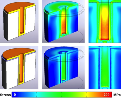
Simulated distribution of thermal induced stress in different TSV designs. The top row shows a TSV with thin annular metal lining (d = 10 µm). The middle row depicts the thermo-mechanical buffering influence of a thin (d = 5 µm) BCB polymer lining between the metal and silicon matrix. In both cases the thermal induced stress is investigated at 100°C for TSVs with a via diameter and via depth of 50 µm and 150 µm, respectively. Courtesy of EV Group.
Process Issues
Things can go wrong during assembly, especially if the different parts come from different foundries and this creates a number of issues that have yet to be resolved. Semiconductor Engineering wrote about the turf war going on between the semiconductor manufacturing companies and the outsourced semiconductor assembly and test providers (OSATs) who have dominated IC packaging and testing to date. But it may be easier for semiconductor companies to move onto the OSAT turf than the other way around; although they may want to retain the margins they are used to making rather than the smaller margins of the OSATs.
“Different carrier technologies, such as temporary bonding can be used, but then who does debonding,” asks Uhrmann, “Thin chip handling has been an issue. Until these types of issues are resolved, we are likely to see semiconductor companies wanting to do this in-house.”
Another aspect of the process involves the EDA tools necessary to create this kind of system. “The EDA industry has undertaken a cooperative research effort which has led to 2.5D-IC design and verification flows qualification at TSMC, GlobalFoundries, etc.,” says Casale-Rossi. “However, it is too early to answer if additional tools will be necessary and this will be driven by customer requirements and business considerations.”
Others see the need for new tools, particularly in the areas of modeling and analysis. A recent book “Design and Modeling for 3D ICs and Interposers” by Madhavan Swaminathan and Ki Jin Han (full review to be provided) sheds light on many of the modeling aspects of TSVs. “Consider the electrical response of TSVs, which are defined by their physical dimensions such as diameter, height, oxide thickness, pitch, shape (cylindrical or tapered) and by the materials used (copper, tungsten, oxide and silicon). These structural and material properties not only affect their electrical response but also affect their mechanical and thermal behavior.” The concepts contained in the book are being commercialized by E-System Design.
Standards
provide a foundation that can focus the efforts of many people and organizations. But when standards are created too early they can stifle innovation. “Standards need to emerge and be proven in the marketplace,” says Janac. He points to Wide I/O as an example of an emerging SoC standard for DRAM integration. However, it appears that this may not be ready for adoption yet, as reported in Tougher Memory Choices in June.
Another standard being developed for 3D testing enables access to devices within the middle of a stack. While not strictly necessary for 2.5D, such a standard would enable disparate test structures to be connected together so as to present a coordinated approach on the external pins of a 2.5D structure. The IEEE 1838 working group is currently developing this standard.
Tipping point
“Volume would cause the costs to be squeezed out of the creation and integration of the interposer,” says Uhrmann. “Most producers have pilot lines up and running and they all seem to be waiting for someone to turn the switch. When the first one does, the industry will follow, and then there will be pressures to reduce the prices. So, the question is what will trigger the volume? It must have enough volume and it must need the technology. When someone says we actually need it, then the whole industry will change.”
Janac agrees. “Volume applications need to drive the market. Some possibilities include application processor coupled to a modem for high-end mobility, analog/digital for consumer, processor coupled to FPGA for automotive and server or CMOS sensor coupled to an application processor for DSLR and high-end smart phone cameras.”
But none of these define an actual need. “This is a security issue,” says Bernard Murphy, chief technology officer at Atrenta. “People are hacking the external interface of the memory, and there are companies pipelining AES cores in the DDR banks so that the data is encrypted between the memory and the processor. If you go to a 2.5D or 3D architecture, then you no longer have to do this.”
“Cost is not a limiting factor right now for applications such as the IoT,” says Drew Wingard, chief technology officer at Sonics. “Since 2.5D can improve the form factor and reduce power consumption, it will be attractive for IoT applications in the wearable and other very low power applications. These applications require the integration of diverse sensor, wireless and computing technologies that are not suitable for single-die integration — both from a process technology and a design cost perspective.”

 |
|
 |
 |
 |
 |
 |
 |
 |
 |
Brian,
E-SD has commercialized and released our 3DPF V3.0 at this year’s ECTC conference in Orlando. After working with many large companies and their valuable feedback on V1 and V2, we felt V3.0 was ready for the masses. Please contact me if you want to have an evaluation copy. Very easy and intuitive to use.
Late October (EPEPS conf), we will release an upgrade module for additional functionality that was requested by several companies.
regards,
Bill
A good, balanced article, need more such to clear the hype and fog created by amateur Bloggers eager to make a fast buck with 2.5 – d / 3-d die stacking, a technology that still needs to resolve several fundamental technical concerns before prattling on about design and supply – chain issues.
A suggestion for Brian, how about a few more articles on 2.5-d and 3-d stacks, but cover electrical performance, process and reliability issues in some depth. Find and talk to technical people, not more bloggers or marketers.