Silicon health becomes much more complex for stacked dies with limited probe access.

Ever since the earliest semiconductor devices, silicon health has been a concern. Systems manufacturers wanted to be sure that their chips worked properly before being soldered onto printed circuit boards (PCBs). They put pressure on semiconductor suppliers to test wafers, individual dies, and assembled parts before they were shipped. A wide range of design-for-test (DFT) approaches were developed to make test quality better and faster. While testing traditional 2D chips has not always been easy, two trends in the industry are making test much harder.
The first major evolution is the ever wider use of chips in mission critical applications, many of these in challenging operating environments. Whether in space, a battlefield, a nuclear power plant, or a self-driving car, sudden chip failures can lead to catastrophic results. This puts even more pressure on manufacturing quality, but that’s not enough. Effective silicon lifecycle management (SLM) is also required, with proactive in-field monitoring to detect signs of silicon aging, environmental extremes, and potential failures before they happen.
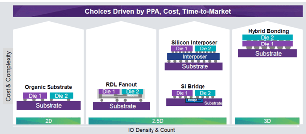
The other trend is the increasing adoption of multi-die technology for 2.5D and 3D packages. There are many advantages to placing multiple dies on a single interposer and stacking dies vertically with through silicon via (TSV) connections. More functionality can fit in the same PCB footprint, interconnects are faster, different chip technologies can be mixed within a single package, and it’s much easier to develop successor products and variations for new applications. However, silicon health becomes much more complex, especially for stacked dies with very limited probe access.
These two trends are converging: multi-die designs with advanced SLM content are appearing in some of the most demanding applications. The need for monitor, test, and repair (MTR) has become critical. Silicon health must be monitored at every stage of the silicon lifecycle, including mission mode in the field. In addition to passive monitoring, proactive test and repair is required during manufacturing, power-on, and power-off, with checking at periodic intervals during field operation. Repairs must be made in place whenever possible. MTR has implications for many stages of chip development and deployment.
Manufacturing individual dies (also called chiplets) in multi-die design is similar to 2D chips, although the higher I/O density presents some challenges. Wafer sort identifies each known good die (KGD), with test enabled by dedicated or shared test ports, built-in-self-test (BIST), and other monitoring mechanisms. SLM helps to optimize power, performance, and area (PPA) of the design and to maximize production yield. Some types of faults detected at this stage can even be repaired, for example with memory redundancy.
The die-to-die interconnects must also be tested, followed by further system-level test and repair to determine each known good stack (KGS). Once stacks are assembled into packages, final manufacturing test can be performed. Additional MTR requirements arise in the field to ensure reliability, availability, and serviceability (RAS). Degradation monitoring helps to ensure reliability. Availability is improved by in-field reconfiguration and repair, for example on die-to-die interfaces with redundant lanes. Finally, remote debug and diagnosis enhance serviceability.
SLM IP lies at the heart of both manufacturing and in-field silicon health. Typical IP types include sensors, BIST, functional safety, and monitors for paths, delays, and signals.
Synopsys provides a wide range of test and SLM solutions for multi-die systems that meet or exceed all the requirements discussed thus far. SLM IP offerings include:
The figure below shows an example of a typical multi-die design, including where Synopsys SLM IP should be used.
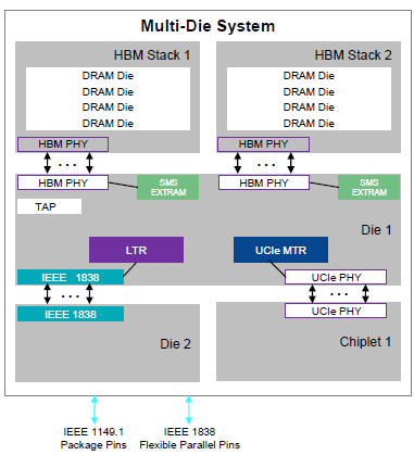
The solution supports the IEEE 1838 DFT access architecture standard to test both individual dies/chiplets as well as the die-to-die interconnects between them. This solution integrates with the Synopsys SHS hierarchical test solution for efficiently managing designs using multiple test and SLM IPs. Lane Test & Repair (LTR) IP provides in-system BIST for high-volume lanes, including reconfiguration and repair using redundant lanes. Signals are shifted from the faulty lane to a spare lane on both dies, and the faulty lane output is placed in standby mode.
Most multi-die designs use the Universal Chiplet Interconnect Express (UCIe) for die-to-die interconnects. Synopsys IP supports the UCIe standard and offer a companion IP, Synopsys MTR, with capabilities including at-speed inter-die lane BIST, signal integrity monitoring, and repair of interconnects, as well as multi-die DFT and SLM access
One of the major benefits of 3D design is that memory dies can be stacked for a highly dense solution. Synopsys SLM EXTRAM IP supports all popular logic-to-memory physical (PHY) standard protocols, including High Bandwidth Memory (HBM) and double data rata (DDR) interfaces. This IP provides at-speed interconnect test and repair, programmable at-speed external DRAM BIST, and system-level calibration. For repairable memories, SLM EXTRAM also performs incremental memory repair over the full silicon lifecycle.
Recently, Synopsys and TSMC collaborated on a 3nm (NP3) test die to develop a multi-die MTR reference flow and demonstrate a silicon proof point for the combined solution. The 3D chip design includes two copies of the same die, interconnected by UCIe via CoWoS interposer. The UCIe I/O signals are placed so that the channels align when the two dies are flipped with respect to each other. The die-to-die I/O signals are placed on either side of the UCIe interface so that the inputs and outputs of each die align with the outputs and inputs of the other die.
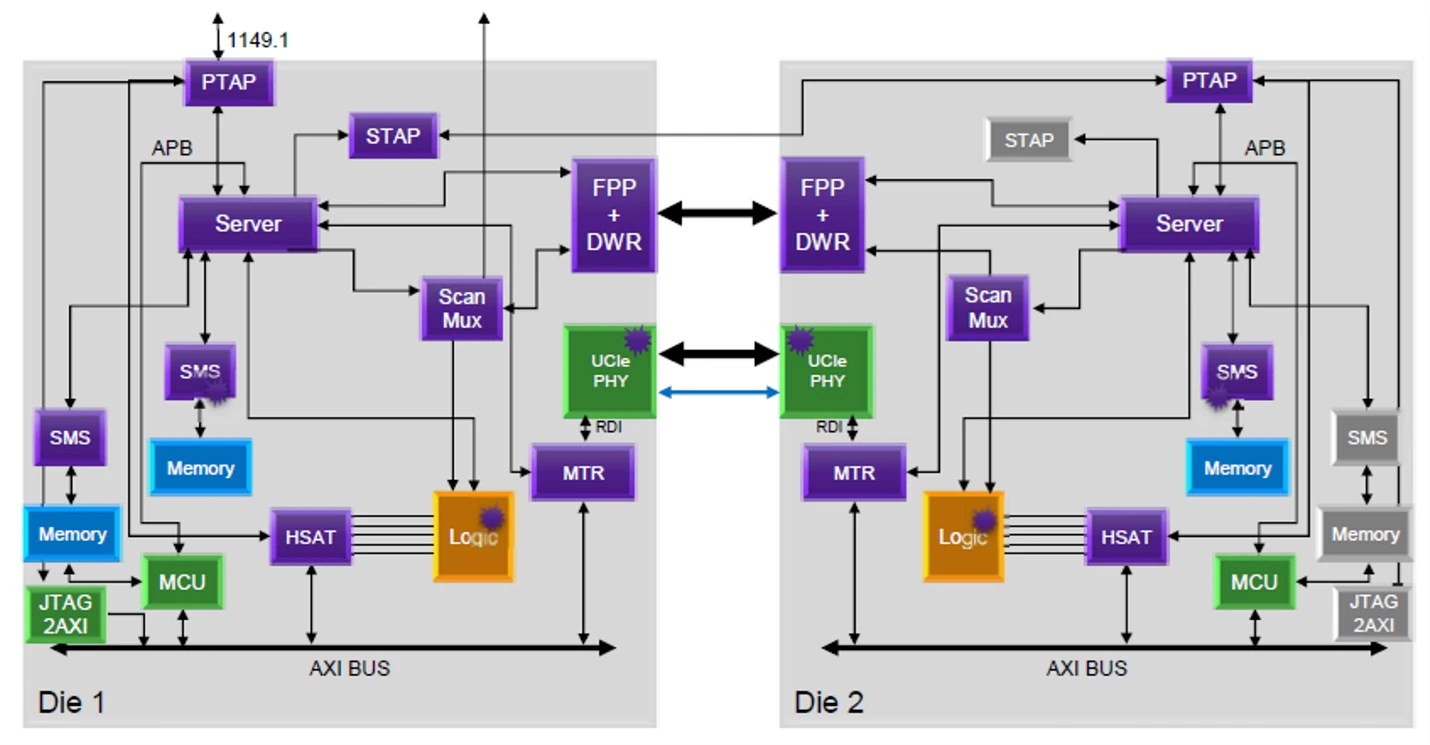
The Synopsys IP in the figure above includes SMS and CDM for embedded memory test, monitoring and repair; a die wrapper register (DWR) and flexible parallel port (FPP) to support multi-die IEEE 1838 DFT; and High-Speed Access & Test (HSAT) along with SF/SEQ for intra–die logic test. HSAT is crucial since only Die 1 has its test interface connected off-chip. From the system or tester perspective, Die 2 is “shadowed” behind Die 1 and so all test of Die 2 must be performed with the help of resources in Die 1.

This project was judged to be a complete success. The multi-die system worked at first silicon, and demonstrated that the silicon, interposer, IP, and tools are all ready for multi-die design. The results of this collaborative project will be presented at the 2025 TSMC Open Innovation Platform (OIP) Ecosystem Forum. A link to the online presentation will be available on October 9.
The two key trends of SLM and multi-die design are intersecting for many of today’s advanced applications with high safety and RAS requirements. Traditional test quality and yield methods are being supplemented with MTR technology to improve every phase of the silicon lifecycle. Chip developers need not fret: a robust, silicon-proven solution is available today.
 |
 |
 |
 |
 |
 |
 |
Leave a Reply