Smart software finds more EUV stochastic defects and missing vias, improving wafer yield.

Leading chipmakers TSMC and Samsung are producing 5nm devices in high volume production and TSMC is forging ahead with plans for first 3nm silicon by year end. But to meet such aggressive targets, engineers must identify defects and ramp yield faster than before.
Getting a handle on EUV stochastic defects — non-repeating patterning defects such as microbridges, broken lines, or missing contacts — is at the heart of this challenge. That requires robust, high-throughput inspection strategies to detect and remedy common problems, such as missing vias.
Yield engineers regularly identify critical areas on chips that require targeted inspection. “The inspection recipe plays a key role in determining which defects are detected and how many are detected,” said Satya Kurada, vice president of marketing at KLA. “Twenty years ago, an operator would have set up two care areas for a logic die – one for the random pattern and one for the SRAM region. Today, our inspection systems use patented technologies to automatically generate billions of very tiny care areas based on user-defined patterns of interest.”
Plunging into EUV lithography
One of the fab’s most significant yield and cost drivers is the net number of extreme UV (EUV, 13.5nm) mask layers. EUV photolithography was introduced in 7nm fab lines for the most critical layers, but at the 5nm node, perhaps 75% of the total layers (more than 50 in logic devices) require EUV patterning. The most common random defect, using 193nm exposure or EUV, is the stochastic printing failure.
“Microbridges are not clearly distinguishable from the traditional defects, which come from the photoresist or process tools. Hence, efforts to eliminate the traditional defects are being made in parallel to reduce them by designing new photoresist or improving dry etch process,” said Ki Chul Park, vice president of Samsung Electronics, who talked about manufacturing strategies for 5nm devices at IITC [1]. “The biggest contributor to the total cost is the number of EUV layers used for the patterning of fine-pitch metal and via layers. Roughly 1% to 2% total cost is increased when a EUV layer is added [2], which means that adding an EUV layer has to lead to more than 1% to 2% area reduction.” Park noted that the leading EUV photoresist is capable of single exposure printing of 30nm metal pitch lines with manufacturing-worthy defectivity.
Chemically amplified resists (CARs), which have dominated the industry for decades, are now being challenged by new metal oxide resists (MORs). The advantage of MORs, pioneered by Inpria, a JSR company, is they absorb EUV better, so they can be thinner than CARs and not as likely to suffer from pattern collapse. Other options are emerging, as well, including non-CARs spin-on resists, and dry resist deposition and removal processes from Lam Research. Interestingly, the volume of photons produced by EUV scanners is about 1/14th that produced by ArF (193nm) scanners, which together with finer features explains the intense R&D among Imec, ASML and photoresists makers JSR, Shin-Etsu Chemical, and Fujifilm, as well as processes for photoresist coat/bake/development processes by TEL to extend EUV patterning capability.
Addressing stochastic variation
Stochastic defects are any random, isolated defects that cause such problems as microbridging, locally broken lines, and missing or merging contacts. The loss of line-edge fidelity is called linewidth roughness (LWR) and line-edge roughness (LER). In lithography, critical dimension (CD) non-uniformity can be local (one line to another) or global (across the wafer), and may be caused by reticle error, scanner error, or error from etch and deposition. Overlay error is error in alignment between features. If an edge placement error (EPE) is off enough, shorts between metals can occur, or tiny vias can disappear altogether, causing an electrical open.
“Chipmakers have to differentiate between stochastics, meaning they scale somewhat equally, and systemic defects, meaning there is something about the particular design that makes it vulnerable,” said Aki Fujimura, CEO of D2S. He added that chip manufacturers at the leading edge must resolve sources of systemic variation, and also control the random (stochastic) defects to a level deemed acceptable for high volume production.
Stochastic patterning defects are a big deal. “This is a multibillion-dollar problem because stochastics are becoming a much larger percentage of the fab’s edge-placement error budget,” explained Ed Charrier, CEO of Fractilia. “Stochastics have always been there, but they were a really small percentage of the feature size, so we’ve been able to ignore them until recent nodes,” said Chris Mack, CTO of Fractilia. At the 22nm node, stochastic defects made up 5% of edge placement error (EPE) budget, but at 5nm, it’s 40% of the overall EPE budget, climbing to 50% at 3nm, and on. To make matters worse, the very low volume of photons reacting in the resist — referred to as EUV shot noise (analogous to shotgun pellet dispersal) — of 4 to 5 photons, can increase line-edge roughness.
“Whether you have 4 or 5 makes a big difference,” said D2S’s Fujimura. New EUV processes, including advanced photoresists, focus on improving the quantum efficiency of CAR resists to speed EUV throughput while minimizing stochastics. In CARs, each incoming photon de-protects more than one resist molecule (chemical amplification). Increasing quantum efficiency means either a larger fraction of available photons lead to photoacid generation events, or each photoacid molecule de-protects more resist molecules, or both. Photon-induced variation and the conversion of scarce EUV photons into imaging events leads to higher stochastic consequences in EUV.
Quantifying variation
Stochastic defects fall into four categories (shown in figure 1): line-edge and line-width roughness; CD non-uniformity between features; overlay errors; and feature edges that are too close together (causing shorts) or too far away (causing opens).
“All of these things can impact device performance, yield and reliability, said Fractilia’s Mack. In the lithography cell, optical inspection tools are complemented by the much slower scanning electron microscopes (SEMs), which measure CDs or provide in-line defect review and classification. CD-SEM imaging results contain the actual roughness of printed lines and spaces but also roughness due to SEM noise. Mack explains that traditional image processing filters will average roughness and not reveal actual roughness. “We developed our tool to operate in the frequency domain rather than a spatial domain and we look at how much roughness there is in long length and short length scales using the power spectral density,” he explained. “We might measure 4.3 nanometers of metrology noise on top of actual variation happening on the wafer, but with processing that subtracts the metrology noise, we might get only 1.3 nanometer of roughness,” he said. The tool then models the pattern backward to see what the actual image on the wafer is. The model forward then backward allows a capture of all stochastic defects in a single analysis. It also provides engineers with a method to optimize SEM use, enabling tool-to-tool matching, even with tools from different vendors.
Fractilia’s tool also speeds SEM throughput. Like a television image, SEMs use raster scanning to average several frames (4 to 32) to produce the final image, so a higher image resolution incorporates more frames but extends measurement time. Fractilia’s tool allows an optimization of frame rate for higher SEM throughput at a given measurement precision (see figure 3), which the engineer selects for a given process layer. Because fabs typically have multiple SEMs on the production floor (made by KLA, Applied Materials, Hitachi, others), the software tool also improves SEM-to-SEM matching for improved process control.
A study by Imec using Fractilia’s tool showed a correlation between stochastic defects on 40nm contacts and linewidth roughness [3]. In other words, LWR functions as a proxy for stochastic defects in manufacturing. Mack adds that roughness measurements are not just critical in manufacturing but also in R&D environments where new photoresists are being evaluated. “There may be 20 materials to choose from and companies are running a lot of wafers and measuring CDs to see which produces the better depth of focus and which provides the better roughness. Often, the difference in roughness could be 10%, but different materials could have properties that impact roughness by 10% or 20%. Is the difference between the resists or due to the SEM? This is a major problem,” he said. “Instead, we can remove the SEM noise and compare the materials.”

Fig. 1: Stochastics include defects related to line-edge/linewidth roughness, CD non-uniformity, overlay (alignment) errors, and feature defects. Source: Fractilia

Fig. 2: For this data, the MetroLER software provides an optimum SEMs capture rate that balances precision, accuracy and throughput at around 10 frames. Source: Fractilia
Capturing missing vias
With via counts numbering in the millions, or even billions on advanced logic chips, accurately capturing missing vias or contacts is a significant challenge for yield engineers. The suppliers of optical inspection tools have updated their tools and software dramatically in recent years to detect an increasing number of ever-smaller defects and characterize them more rapidly using smarter (AI-enabled) software. The inspection tool “recipe” (setup for a given process layer), includes such options as:
KLA’s Kurada said an additional parameter on the company’s broadband plasma (BBP) optical patterned wafer inspector is the tunable wavelength bands (deep UV to infrared), which can enhance the signal-to-noise ratio on different films (photoresist, metals, low-k dielectrics, etc.)
But how do engineers determine care areas for a given device? It turns out, two methods are typically used. The first uses known defect or nuisance locations based on history. The second identifies locations from the IC design file (e.g., GDSII) using known weak points or areas of the design with at-risk features, such as dense thin lines. The software then takes all the patterns of interest and automatically generates care areas.
For example, KLA and IBM Research engineers recently developed a binning technique based on repeating arrays that correlates missing via defect inspection data with wafer location. [4] The engineers identified previously missing vias that had not been captured with the previous tool, and they traced the problem to a specific region on the wafer, which indicated a problem with reactive ion etcher (RIE) step.
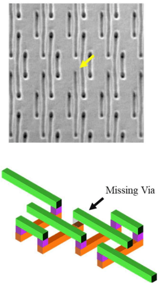
Fig. 3: Missing vias between interconnect lines are a crucial defect for after-etch inspection monitoring. Source: KLA, IBM, IEEE ASMC
In this study, IBM and KLA engineers developed a reliable process control method for in-line capture of missing vias in BEOL logic devices. [4] The engineers used KLA’s inspection methodology to define care area in design (around each via) on via chains patterns at RIE in order to improve capture sensitivity for missing via defects. Care areas were inspected using a broadband plasma (BBP) optical inspection tool and defects were then characterized on an SEM review tool, which bins the defects by type (missing via versus nuisance defect, in this case). Test structures are based on the smallest repeating pattern where inspection sensitivity should be highest.
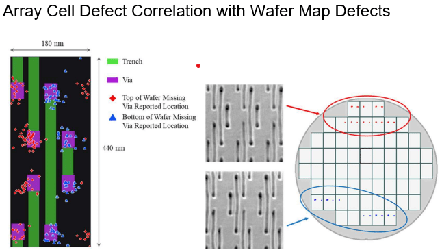
Fig. 4: Cell level defects on the left side of via chain pattern show up as defects at wafer top, whereas missing vias on right side identify all-new defects missed by former inspections. Identified patterns become the basis for in-line monitoring after etch. Source: KLA, IBM, ASMC
The results showed a cell-level signature (see figure 4, repeating cells superimposed), where missing vias on the left side of the via chain showed up exclusively on the wafer top, whereas missing vias on the right side correlated with the wafer bottom. The team suspects the missing via defects were caused by a previously via etch being blocked due to pattern misalignment. The defects on the wafer bottom were not detected by the previous inspection method, which means the strategy can be used to select a representative sampling rate for more effective in-line defect monitoring of missing vias in production. “The inspection results from a BPP system, including binning information, provides actionable data to process engineers so they can make informed decisions in line,” said Kurada.
Defect review alternatives
Yield ramping and yield excursions are nearly always controlled using optical inspection systems and SEM review, but there are cases where other techniques better fill the bill. “Random defects on the order of 20nm are becoming harder to classify, and where AFMs are particularly helpful is when topographical data is needed, to detect dishing and erosion data after CMP, for instance,” said Igor Schmidt, director of operations at Bruker. He noted that while atomic force microscopes (AFMs) tend to have the reputation of low throughput, they can monitor 340 sites per hour for process control of lithography, etch, or CMP processes.
Atomic force microscope (AFM) review tools can take wafer maps data from optical systems, drive to the defect of interest (x,y,z and rotational position using machine vision) and scan across a 30 x 30µm area to image the defects. The defect image shows size, 3D with maximum height (z) information and stickiness. “It’s like when you step on chewing gum versus stepping on a stone. In this case, if we have a defect with large topography and large adhesion, it can be indicative of organic particle or polymer that dropped on the wafer. On the other hand, if you have large topography and weak or no adhesion, this is more likely a particle, maybe a silicon particle or splinter. If you have a hole and no adhesion, it could be a stacking default or crystalline defect, or if you have no particle but adhesion, this could be indicative of oil and a problem in a machine somewhere. So it is a powerful technique to classify defects,” he said.
Packaging, intelligence, yield
One of the most costly yield hits for IC companies doing heterogenous integration is bump yield. In an analogous manner to the dense vias connecting copper wires on the IC, metal bump interconnects are increasingly dense. At the same time, advanced packaging technology enables a variety of 3D schemes, which chip makers are exploiting.
“There’s so much stacking going on right now, which delivers many benefits, but at the same time the number of bumps has exploded. When we talk to the fabs, their number one pain point is delivering 100% inspection of bumps cost effectively,” said Subodh Kulkarni, president and CEO of CyberOptics.
Kulkarni noted that with millions of bumps and automated optical inspection throughputs, rates of 10 to 15 wafers per hour (300mm) are not sufficient. “The sweet spot is delivery of 25 to 30 wafers per hour with 100 million bump capability on a tool with a sub-$1 million price point. Because this is where they’re losing a lot of yield today,” he said.
Optical inspection of copper bumps involves measuring co-planarity, detecting outliers (taller than the tallest spec, or shorter than the shortest spec), bump location and size, but also defects on the bumps. “For outliers, the customer want us to store that bump image, but also determine whether there’s a crack or we see some contamination or part of the bump has been carved off, for instance.” All this information is important.

Fig. 5: MRS optical inspection images indicate the shape, size and potential defects on copper bumps and pads, as well as height profile. Source: CyberOptics
Conclusion
Yield ramping for advanced 5nm devices or in advanced packaging, requires identification and removal of key defects at lithography through to packaging materials, making smart and fast wafer-level inspection essential.
Stochastic defects become an increasingly bigger problem from 22nm to 5nm and can significantly affect device yield and reliability. Engineers are using new tools to identify and subtract stochastic defects – while enabling more accurate SEM review, tool matching, and improved SEM throughput in fabs. Combining design-aware software with optical and e-beam review tools can improve the capture of hard-to-image yield killers like missing vias. High throughput, 100% wafer inspection of copper bumps is key to high yield in advanced packaging.
References
[1] K.C. Park and H. Simka, “Advanced Interconnect Challenges Beyond 5nm and Possible Solutions,” IEEE International Interconnect Technology Conference (IITC), 2021.
[2] B.S. Kasprowicz, et.al., EUVL Workshop, 2017.
[3] D. De Simone, “EUV Materials Status at Imec,” Imec PTW, April 2019.
[4] G. Jensen, et.al., “Missing Via Defect Capture Enhancement Using a Novel, High-Precision Array Segmentation Inspection Technique,” IEEE Advanced Semiconductor Manufacturing Conference (ASMC), 2021.
Related Stories
Finding, Predicting EUV Stochastic Defects
AI in Inspection, Metrology, And Test
Fundamental Shifts in IC Manufacturing Processes

 |
 |
 |
 |
 |
 |
 |
Leave a Reply