It’s hard to predict when DRAM will run out of steam, but two new technologies hold promise as replacements.

Memory — and DRAM in particular — has moved into the spotlight as it finds itself in the critical path to greater system performance.
This isn’t the first time DRAM has been the center of attention involving performance. The problem is that not everything progresses at the same rate, creating serial bottlenecks in everything from processor performance to transistor design, and even the technology to manufacture these devices. It’s now memory’s turn.
“Memory systems are at the forefront again for bottlenecks,” says Frank Ferro, senior director of product marketing for IP cores at Rambus. “AI is driving a massive need for memory capacity and bandwidth.” Scaling, packaging, and even radical bit-cell innovations may be needed to keep the DRAM market humming along.
To sate our appetite for memory, scaling today’s DRAM to smaller dimensions to increase capacity is an obvious tactic. But DRAM may run into scaling limits. If it does, new approaches will be needed. That said, DRAM’s end of scaling has been predicted — incorrectly — before. “Over 10 years ago, the ITRS roadmap said 90nm would be it for DRAM. Now we’re at 16nm (1z),” says Jim Handy, general director of Objective Analysis, referring to the “1z” notation used to describe DRAM process generations.
Several flavors of DRAM exist that appeal to different applications, even within AI. For ML training, HBM is the memory of choice. That’s a more-than-Moore approach, which stacks separate memory dice to create a single unit with greater capacity. It’s relatively new, and there’s a price for that capacity, but makers of ML-training hardware have been willing to pay the price.
In addition to plain DDR memory, there’s also GDDR, originally for graphics, and LPDDR, for lower power. Those last two are being leveraged in applications like edge inference and advanced driver-assist systems (ADAS) in automobiles, looking for a balance in capacity, latency, bandwidth, power, and price.
“There have been a dozen or so characteristics that make DRAM attractive, including symmetric read/write times and power and infinite endurance,” says Steven Woo, a Rambus fellow and distinguished inventor.
Those benefits join a few others as the most obvious reasons to use DRAM:
These characteristics create a high bar for any other technology or approach that wants to challenge DRAM. “It’s a staggering technology for the price it’s sold at,” says Marc Greenberg, IP group director of product marketing at Cadence. And yet what happens if DRAM stops scaling? Will some of those advantages be lost over time?
DRAM scaling
At the heart of all DRAM variants is the basic DRAM bit cell — a capacitor. “DRAM is basically an analog circuit. Those don’t shrink as well as digital circuits do,” says Greenberg. To scale to a smaller size means to shrink the size of the capacitor. That leaves fewer electrons on each capacito, which makes for a less robust bit-cell state. So the trick is to find a way to put more electrons onto a capacitor that takes less floorspace.
One of the first changes to make this possible was making a vertical capacitor instead of a horizontal one. That put the primary surface of the capacitor in the vertical direction, and it could grow without impacting area on the surface of the chip. But that growth has limits. Even now, the aspect ratio for a DRAM bit cell is as much as 30:1, according to TechInsights Fellow Emeritus Dick James. For comparison, Rambus points out that the Burj Khalifa in Dubai has a 6:1 aspect ratio — a mere fifth of what DRAMs use.

Fig. 1: The Burj Khalifa skyscraper in Dubai. Source: By Donaldytong – commons:File:Burj Khalifa.jpg, originally from the author.
As the bases of these conical cylinders shrink so that more can be packed onto the chip, the height has to increase to maintain the same capacitor surface area, pushing the aspect ratio. “Very-high-K dielectrics could take DRAM further [by increasing the capacitance per area], although the materials are harder to manage,” says Handy.

Fig. 2. Simplified DRAM bit-cell capacitor, not to scale. Advanced aspect ratios could be twice what’s illustrated here. Source: Bryon Moyer/Semiconductor Engineering, based on description by Rambus
DRAM has pushed past many of the forecasted limits, and, so far, that continues. Basic scaling is forecast through the 1γ (gamma) node that’s in development now, according to Handy. With 1α and 1β ahead of that, and with 1.5 to 2 years between nodes, that takes us out about 6 years. And HBM also provides greater capacity with a given bit cell. As costs drop on the stacking technology, that also can help to extend DRAM’s life.
Capacity aside, bandwidth is the other major need. Rambus’ Woo says that speed has been doubling every 5 to 6 years. While that helps to extract the contents ever faster, it also makes the wiring more delicate to design. Signal integrity is now an important issue for signals inside and outside the memory. In addition, that data rate also poses a power challenge. For ML systems in particular, data movement is a major contributor to power, so greater bandwidth must be accompanied by efforts to keep power as low as possible.
Architectural techniques also are helping to make better use of the memories we have. Part of this is for cost reasons. Handy says that cellphones have moved away from using NOR flash and SRAM to using NAND flash and DRAM. That makes for a much more challenging design, but the low costs of NAND flash and DRAM make it worthwhile.
While that can increase the use of DRAM, another technique has eaten into the DRAM market. It turns out that greater average latency can be achieved not by adding more fast memory like DRAM, but by adding more slow memory, like flash, behind a fast memory. Handy details the reasons for this in a separate blog, since it’s not intuitive.
All of these considerations notwithstanding, there appears to be no letup in the demand for DRAM, and the question remains as to how far scaling can continue — and what will happen after that.
A new approach to stacking
While HBM leverages current die-stacking techniques, there’s a new stacking approach that purports to have benefits over today’s state of the art. It’s from a company called Tezzaron, and while the technology isn’t specifically related to memory, and Tezzaron isn’t specifically a memory company, they’ve been using DRAM as a development vehicle for the approach.
The challenge with HBM is that wafers are singulated prior to stacking. This is done to ensure that only good dice are stacked. Because of this, the dice must be relatively thick in order to withstand handling as the die is manipulated. Because of this thickness, through-hole vias (TSVs) are used to make connections between the dice in the stack.
While DRAM bit cells are flirting with very high aspect ratios, interconnect tends to top out at aspect ratios around 10:1. In order to maintain physical rigidity, a wafer can’t be thinned down much further than 100 μm, making for a 10μm TSV width. In order to fill such a TSV, copper is needed. Other metals can’t get so far down into the TSV. The challenge with copper is that it has a very different thermal coefficient of expansion (TCE) than that of the surrounding silicon. So when the temperature changes, it can create significant stresses in the silicon — enough stress to alter the behavior of any critical transistors in the region.
For this reason, “keep-out” zones are established around each TSV; circuitry is banned within some tens of microns. Meanwhile, the pitch of the TSVs is also of the same order of magnitude. “These big TSVs force you to a wide TSV pitch, and they have to be located away from circuitry,” says David Chapman, Tezzaron’s chief marketing officer.
Tezzaron’s approach operates at the wafer level rather than the die level. The first two wafers are mated face-to-face using copper-to-copper hybrid bonding. “The oxide bond forms first and provides the mechanical bonding pressure to produce the metallic copper bonds. The coolest feature of this method is that the oxide bond is weak (temporary) before anneal, allowing an alignment check and rework if the first attempt proves unsatisfactory,” says Chapman. This technique uses no fillers, solder, or adhesives. A molecular bond is formed between the SiO2 on both wafers and the copper interconnect on both wafers.
This first bonding step yields a two-wafer stack. One side of that stack — the backside of one of the original wafers — is then ground to a thickness of about 10μm. This would be very mechanically unstable except that the thinned wafer has been bonded to the thick one, keeping it sturdy. According to Tezzaron, the grinding has no impact on the integrity of the bond.
This can be repeated with another two wafers, producing two two-wafer stacks. The two thin sides of the stacks then can be bonded together (with respect to the original wafers, this would be backside-to-backside) to create one four-wafer stack. This process of grinding and further stacking can be repeated as desired. Once they are all in place, the wafer sandwich can finally be singulated, yielding dice that are now thick enough to be mechanically stable. A four-die stack can end up being the same thickness as a standard die.

Fig. 3: The stacking process starts with (a) bonding two face-to-face wafers into (b) a single, molecularly bonded unit, and then (c) grinding one side down to expose the SuperContacts. Two such units can then (d) be bonded back-to-back to create (e) a single four-wafer stack that’s the same thickness as a standard wafer. Source: Bryon Moyer/Semiconductor Engineering.
While the connections between the face-to-face dice are obvious, connections also are needed between the backside-bonded dice. Those connections are made with TSVs on a thick die, but, because these dice are so thin, they can be made with what are essentially slightly bigger vias. Tezzaron calls them “SuperContacts.” A 10:1 aspect ratio on a 10μm-thick die would give a 1μm-wide via — much narrower than a TSV. And because the contact is so shallow, copper isn’t needed. Tungsten can be used instead. Tungsten is much more thermally compatible with silicon than copper, so keep-out regions are no longer needed. And the pitch between these vias can be as low as 3μm.
This means that SuperContacts can be put anywhere on the die — including within circuits. The result is that, depending on the needs of an application, there can be 100 to 1,000,000 times more connections using this technique than is possible using TSVs. In addition, because this becomes one large molecularly bonded die, heat from the inside can travel out through the entire mass, not just through TSVs and metal thermal pipes.
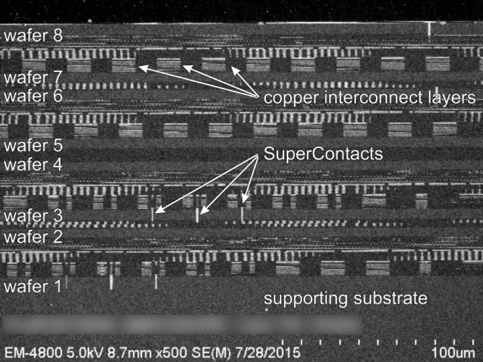
Fig. 4: SEM of a bonded stack of 8 wafers, each of which uses 10 layers of metal for a total of 80 layers. Source: Tezzaron
By bonding wafers, it’s no longer possible to work only with known-good dice. So yield becomes a bigger consideration. According to Chapman, “There are no 100% good dice — they all need repair.” As long as the quality of the dice remains within the repairable range, reasonable yield can be achieved. Because so many SuperContacts can be created to communicate between dice, repair schemes need not be limited to within one die. He contends that, unintuitively, the more wafers one stacks, the more repair opportunities there can be, improving yield.

Fig. 5: Yield improving with the number of layers. Source: Tezzaron
How the wafers are allocated in the stack is partly an architectural question. You could have bit cells on one layer, high-performance logic on another layer, and SerDes interconnects on yet a third layer. In their development vehicle (which they call DiRAM), they put sense amps on a logic process at the bottom and then bit cells on a DRAM process for the upper layers.
It’s possible this could be a next step when the DRAM bit cell stops scaling. As to whether this might be taken up ahead of that point, Chapman acknowledges, “This scares a lot of folks.” Tezzaron has done it on a small scale, but it still has to be proven. Yet because it uses no new equipment and involves no new physics, the barrier to adoption is lower than it might be for an entirely new technology.
A new technology to replace DRAM?
Given a choice between tweaking an existing, well-known technology and taking on something completely new, technologists always will choose what’s known. Higher risks are tolerated only when the easier paths have all come to an end. DRAM technology is mature, and it’s made in extremely high volumes with low costs, creating huge market inertia.
The conventional wisdom is that any new memory technology would need to fit between DRAM and NAND flash — the storage-class memory space. Replacing DRAM completely with a new technology is a much bigger question, even though Handy says that 3D Crosspoint memory (from Intel and Micron) could “put a dent in” DRAM sales.
Developers continue to work on new non-volatile memories (NVMs), but if the goal is to replace DRAM, rather than augmenting it, then most new approaches have had some fatal flaw. He suggests that the industry would have to hit a wall to switch, and one or two large customers would be needed to drive up initial volumes quickly so that costs could drop down to the levels that DRAM enjoys.
Nantero, however, is gunning for DRAM with a new non-volatile technology. Built from carbon nanotubes (CNTs), they call it NRAM (where the N stands for “nanotube”). If it could meet the other characteristics of DRAM — which no other NVM has done yet — then it might have a chance. But this approach has a long way to go to achieve commercial success. Nantero has one licensed customer, Fujitsu, but they’re using it as an NVM, not as DRAM. According to TongSwan Pang, senior marketing manager at Fujitsu, the reason for doing that is not because of the technology itself, but because of the nature of the DRAM market and the experience that many memory makers have had with it.
The technology relies on van der Waals atomic forces for its action. At small separations, the CNTs literally bond together, turning a random mass of CNTs into a conductor between electrodes. When separated apart, that conduction is broken. Electrostatics are used to create the connection, with a voltage bringing them together. The connections are broken by thermal vibrations generated by an opposing voltage. “Adjacent atoms literally bond to each other using van der Waals forces,” says Bill Gervasi, Nantero’s principal systems architect.
While there may be a thick mass of CNTs, only the bottom few angstroms actually switch, making the technique insensitive to thickness. A challenge, however, has been the tendency for the metal at the electrodes to penetrate the space, shorting the cell out. Gervasi says that “IBM and Samsung tried and failed [because of this]; they were trying to get the whole cell to switch.” What Nantero did was to add a second layer of a different kind of CNT. The switching layer is a woven random mass, while the upper layer has CNTs that are aligned to from a mat. That mat acts as a barrier to the metal, protecting the cell.

Fig. 6: A schematic of an NRAM bit cell. The CNT Type 1 is aligned to prevent metal migration into the cell. The CNT Type 2 performs the switching. Source: Nantero.
The CNTs are spun onto wafers during manufacturing and then etched to isolate the individual cells. It’s possible to stack multiple layers of bit cells in a crosspoint array to optimize performance. Tiles are created with a width, depth, and height that achieve the desired performance — in this case, to match DDR4 timing. Their DDR4 device has four layers. Once the tile is designed, it can be repeated to create the desired overall capacity.

Fig. 7: Four-layer crosspoint array. Source: Nantero.
At present, the resistance difference between a set and reset state is about 10:1. They’re working to increase that to 30:1. Shrinking the size of the cell helps, since it increases the resistance and makes it possible to read the cell with less current. They’ve modeled cells down to 2nm width.
The basic cell is a 1R cell (single resistor only), but they can create 1T1R cells with selector transistors as well. The transistors would be located in the underlying silicon, with interconnect up to the CNT bit cells. This gives them a switching speed of 5ns, regardless of memory size. “We could be at 16 times the density of DRAM with the [same] speed,” says Gervasi. They can improve the speed by using a 1T2R cell and sensing the current differentially for applications that need the performance and can tolerate the extra cost.

Fig. 8: A 1T1R configuration, which Nantero says is better for small arrays. Source: Nantero.
While data retention is not a typical concern for a volatile memory, they claim the ability to hold data for hundreds to thousands — even tens of thousands — of years. DRAM does have infinite endurance; Nantero has tested their approach to 1013 write cycles with no wear-out. Some quick back-of-the-envelope numbers say that, if you’re writing 1,000 times a second, then you’d hit this limit in something over 300 years.

Fig. 9: 64-Kb tiles arranged into a 16-Gb memory. Source: Nantero
If this technology proves itself out, it could add an interesting dynamic to the DRAM market — especially as an NVM contender for storage-class memory. (Interestingly, Nantero refers to this as memory-class storage.) Cadence’s Greenberg says that, “It’s a technology that shows promise.” The inertia against displacing DRAM in the short term is substantial, however. The death of DRAM (like the death of CMOS) has been forecast — and missed — too many times before to assume that it’s imminent in the foreseeable future.
Related
DRAM Knowledge Center
DRAM Scaling Challenges Grow
More nodes and alternative memories are in the works, but schedules remain murky.
Tricky Tradeoffs For LPDDR5
New memory offers better performance, but that still doesn’t make the choice simple.
Why DRAM Won’t Go Away
New materials, new architectures and higher density have limited what can be done with DRAM, but it’s still king (Experts At The Table Part 3)
HBM2E: The E Stands For Evolutionary
The new version of the high bandwidth memory standard promises greater speeds and feeds and that’s about it.
 |
|
 |
 |
 |  |
 |  |
Leave a Reply