Design smarter test chips with more Kelvin structures around critical interconnects under development.

As the semiconductor world excitingly explores the potential of new advanced package solutions for their intricate and novel designs, challenges arise from undetected defects caused by the complexity of the designs and the lack of accessibility to the interconnects for testing. This typically results in a long cycle time to achieve yield entitlement. Undetected defects at the development stage can also lead to an exponential increase in the cost of chip failures in the system during high-volume production. This issue can worsen when it manifests as latent reliability issues in the field. The continuous increase in complexity in the advanced package design and the diversity in the physical properties of interconnects aggravate the outlook ahead.
While exciting advancement in optical metrologies such as x-ray fluorescence, atomic force microscopy, ellipsometry, white-light interferometry, and scanning capacitance microscopy along with AI/ML driven analysis have helped engineers to detect defect signatures at the early stage of the package development and during high volume production, there has been little to no advancement in the electrical side of defect detection mechanism. Engineers still rely on test chips with long daisy-chains of thousands of interconnects, resulting in a significant loss of information due to the averaging effect of resistance measurements. To make matters worse, engineers are forced to create additional daisy chains on the board, primarily due to the limited number of tester channels available in the ATEs. As shown in Figure 1, mock outlier resistance measurements caused by hairline cracks in a daisy chain with 1000 interconnects shift the average resistance from 50 Mili-ohms to 50.025 Mili-ohms. This is too small a difference to be detected as an anomalous daisy chain. Since it’s not an open failure, it will not be detected by the continuity test with a large limit. These defects may not be detected even during the package qualification process and can result in yield issues in high-volume production or latent reliability issues.
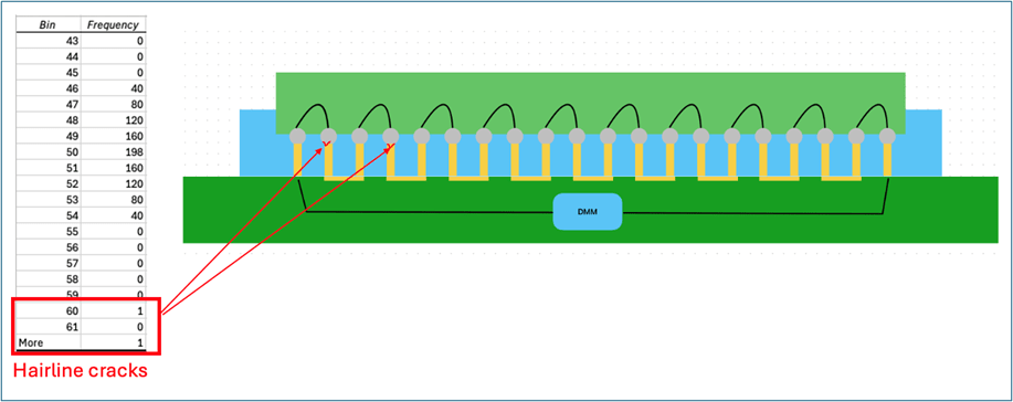
Fig. 1: Traditional daisy chain with hairline cracks (mock data).
Some engineers started adopting Kelvin structures in the test chip for more accurate examination of the critical interconnect structures under development; however, the number of tester channels available still limits the effectiveness of their investigation.
The Modus Test Parametric Tester (MPT) and Modus Test Cycler (MTC), as shown in Figure 2, were initially developed and used to measure the CRES of test sockets using the Kelvin method, ensuring that only known good sockets are used in the test. The increase in package pin counts drove the development of the tester with higher channel counts and the cycler with a higher pusher force, resulting in up to 29,000 MPT Kelvin channels with a micro-ohm range of accuracy and repeatability, and up to MTC 2000 lbs. force capability.
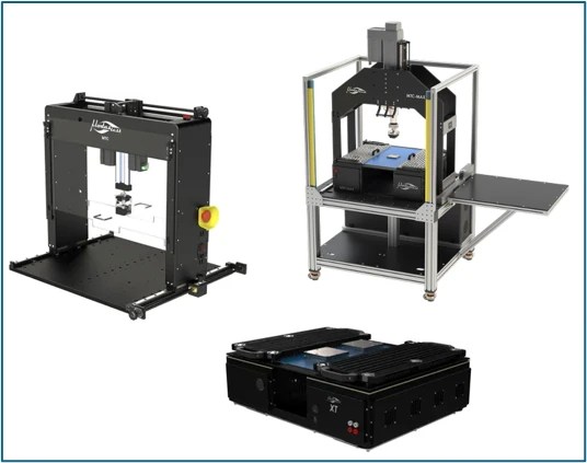
Fig. 2: MPT and MTC series.
With high density and accuracy, MPT/MTC enable engineers to design smarter test chips with more Kelvin structures around critical interconnects under development/investigation, and shorter daisy chains to improve the detectability of defects. As shown in Figure 3, the same hairline cracks can be easily identified as outliers for further analysis, which helps prevent yield issues in high-volume production or latent reliability issues in the field.
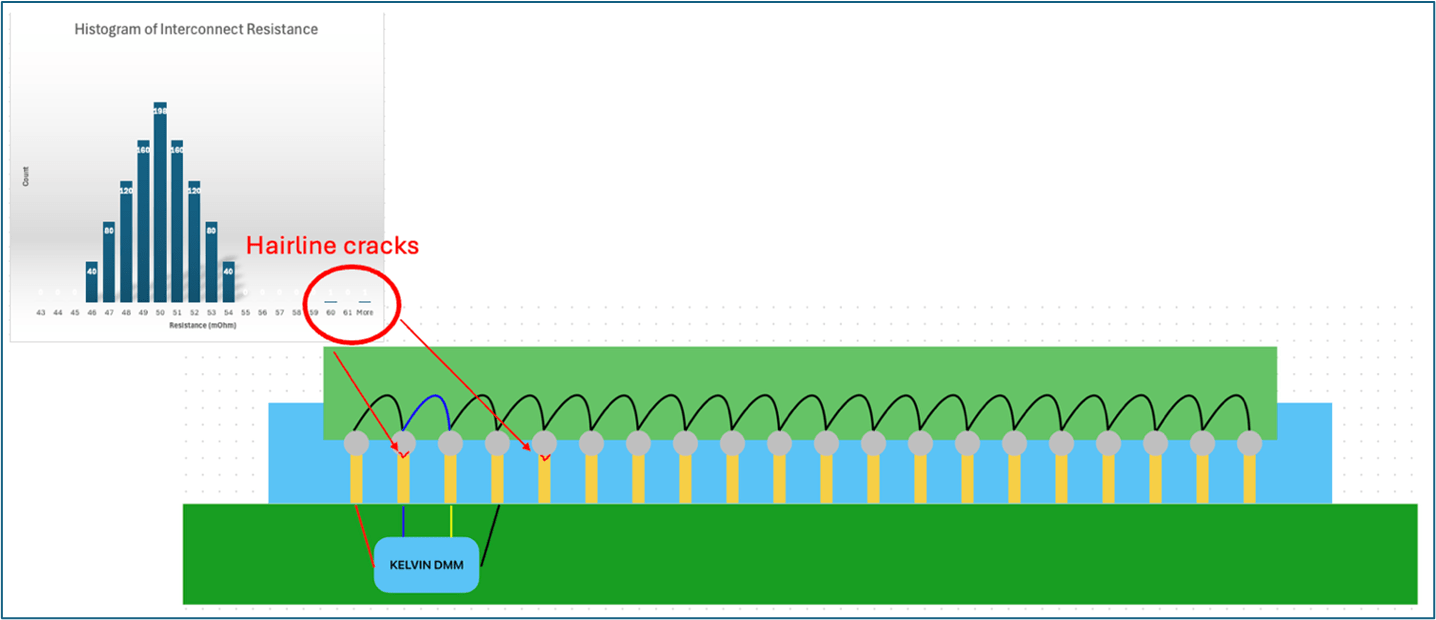
Fig. 3: MPT-enabled characterization (mock data).
The handler-dockable interface of the MPT enables engineers to collect massive data across process corners for further correlation with results from advanced optical metrologies, AI/ML-driven analysis to improve defect signature detection capability, and 3D model verification for continuous improvement of package EDA tools.
Please also refer to the recent video by Jack Lewis, CTO at Modus Test, on this topic: https://semiengineering.com/issues-in-ramping-advanced-packaging/
 |
 |
 |
 |
 |
 |
 |
Leave a Reply