New and faster memory designs are being developed, but their future is uncertain.

As DRAM scaling slows, the industry will need to look for other ways to keep pushing for more and cheaper bits of memory.
The most common way of escaping the limits of planar scaling is to add the third dimension to the architecture. There are two ways to accomplish that. One is in a package, which is already happening. The second is to sale the die into the Z axis, which which has been a topic of discussion for a while.
“3D DRAM is being talked as a concept, and a lot of work is happening in the industry, developing the equipment, developing advanced ALD, selective deposition, selective etch, 2D materials for access devices — they are all happening,” said Naga Chandrasekaran, senior vice president of technology development at Micron. “But there’s not enough to say, ‘Yep, I see it, I can now make my belief and turn it into reality.’”
There are new ways of building a dynamic memory cell that are more amenable to monolithic stacking than the current architecture allows. But most of the effort today is going into stacking multiple DRAM dies as a step that allows the current memory cell, which has experienced years of learning, to continue its dominance. The question is when – if ever – will the alternatives be attractive enough to get traction?
The current DRAM bit cell relies on a tall, narrow capacitor to store charge. If the horizontal dimensions are made smaller, then the radius of that capacitor shrinks, and it must be made yet taller if capacitance is to be kept constant.
Taller capacitors make it harder to manufacture that capacitor correctly and with good yield. While that may work out with continued development efforts, it does raise the question as to whether any fundamental change is needed. Capacitance per bit cell has been going down over the generations, but that merely postpones the ultimate reckoning – if such a reckoning lies ahead.
Two roads to 3D
The most straightforward way to stack DRAM cells keeps the current DRAM technology in place and stacks multiple dies atop each other. This is the advanced-packaging approach used for high-bandwidth memory (HBM). Common HBM stacks are 4- and 8-high, with 16-high expected soon.
Compared to basic DRAM, this is a more expensive approach because of the effort required to stack dies in a package. But for applications that require lots of nearby memory, like artificial intelligence, it’s been worth the cost.
“HBM has, up until now, been limited to some very high-end graphics, high-end computing, and so it’s been a niche,” said Howard David, senior technical marketing manager for memory interfaces at Synopsys. And that has limited the volumes and learning available for the through-silicon vias (TSVs) needed for HBM. “Through-silicon vias haven’t really gotten very far along the learning curve. Artificial intelligence is going to be the thing that pushes it past the threshold to where more money will be spent to improve the yields.”
HBM performance is improving, too. “When HBM started off, the idea was to have a very wide bus, but it would be slow,” said David. “But now, with HBM3 speeds and DDR5 speeds, they’re quite up there.”
Still, there are limitations. “The size of the HBM stack and its required proximity to the processor chip limit the number of stacks that can be attached to the processor,” said Jim Handy, memory analyst at Objective Analysis, in a presentation at the recent Hot Interconnects conference.
Handy presented a new open memory interface (OMI), which is intended to provide near-memory access at faster speeds, while supporting heterogeneous memory architectures. So system architectures could change in the future, opening up what is currently the HBM space to other memories.
There’s also been a cheaper interim approach to full-on stacking. “DDR for 3D stacking was delayed by something called the dual-die package, or DDP,” said David.
DDP is a stack, but with only two dies. The bottom one faces down and the top one faces up, with bond wires connecting the upper chip to the board. Performance isn’t high, but it meets the needs and cost requirements of some applications, so its development actually has slowed progress on full stacking.
Standard bumps and pillars used for stacking dies leave a 30 µm gap between the dies. “With hybrid bonding, the gap between each pair of dies approaches zero, saving a few hundreds of microns in overall package thickness – which will be critical for devices like smartphones and wearable devices,” said Woo Young Han, product marketing manager at Onto Innovation.
Hybrid bonding is still being perfected, however, and it’s sensitive to die-edge defects that can appear during singulation. This results in the need for new inspections after the wafer-sawing process. “DRAM manufacturers are requesting sub-micron defect detection in the back-end packaging area, which is unprecedented,” noted Han.
Stacking memory on a single chip
Monolithic stacking requires completely different approaches. “Monolithically stacked dies are a natural extension with only a small number of additional steps,” said Andy Heinig, group leader for advanced system integration and department head of efficient electronics at Fraunhofer IIS’ Engineering of Adaptive Systems Division. “But this small number of additional steps leads to a lot of difficulties.”
“For stacked objects, the key is building a good capacitor while minimizing interference with adjacent bit cells,” said Rob Aitken, fellow and director of technology on the research team at Arm. “The biggest electrical challenge is likely to be either margining a stacked bit line or designing a stacked solution that doesn’t need one.”
Another practical hurdle is the fact that stacked layers will occur at the back-end of line (BEOL). “The back end of line needs to be processed at low temperatures, and that makes it challenging,” noted Arijit Raychowdhury, professor of computer and electrical engineering at Georgia Tech.
But the biggest challenge is that, because the current capacitor is so deep, it’s not practical to stack multiple layers. That means that a new bit cell is needed for stacking, and capacitorless bit cells have been tough to build.
Several new bit cells have come to light this year, and they all differ in how they work. But they can generally be divided into three basic approaches — cell-flipping, floating bodies, and gain cells.
Taking a page from NAND
There are efforts afoot to modify the standard one-transistor-one-capacitor (1T1C) cell in a way that reflects what’s happened with 3D NAND, namely turning it on its side. Right now, the bit cell is very small from an area standpoint, but the capacitor uses a lot of vertical room. With this new approach, the capacitor would lie horizontally, which greatly increases the area footprint of the cell.
“One would have to stack a significant number of layers in order to compensate for the area consumption of the horizontal capacitor,” said Jin-Woo Han, company spokesperson at Monolithic3D. “Researchers are also investigating higher dielectric constants in order to reduce the length of the storage capacitor.”
Significantly, the proposed stack would use shared patterning in the same way that 3D NAND does, so that each layer doesn’t need its own patterning step.

Fig. 1: One approach to going vertical with the current DRAM cell. On the left is the standard layout of the cell, while the right shows it flipped onto its side. The capacitors are now horizontal, so enough layers are required to offset the increase in the lateral footprint. Source: Monolithic3D
This was attributed to work being done at the major DRAM manufacturers, but two of them declined to be interviewed. Micron spoke generally about the market, but not specifically about its roadmap. So while it’s interesting, it appears to be more than a rumor.
Monolithic3D, meanwhile, is looking into a different version of a many-stack memory. Instead of flipping the DRAM bit cell on its side, it literally is modifying the 3D NAND structure. In the NAND cell, charges are trapped in a nitride layer, with tunnel oxide blocking their exit for long data retention. The idea is that DRAM doesn’t have to worry about data retention the way flash does because that’s what refresh is for.
This approach takes out the tunnel oxide, sacrificing non-volatility. “As long as we are able to retain data for a few seconds in a nominal device, and a few tens of milliseconds for the tail bits, we can still satisfy the JEDEC standard for refresh,” said Monolithic 3D’s Han. “Instead of using a storage capacitor, we’re going to use the inherent charge-trapping layer embedded inside of the gate stack. We are not utilizing tunnel oxide, so the channel is directly attached to the storage node.”

Fig. 2: The left shows a typical charge-trap flash cell with tunnel oxide (the lower blue layer). The right shows the Monolithic3D cell, which is conceptually the same except that the tunnel oxide is removed. Source: Monolithic3D
In the NAND version, the current runs all the way down a resistive pillar top to bottom. Here, the current starts on one metal pillar. Then, at the selected cell, it crosses over to another metal pillar and continues down, with no current diminution due to the low-resistance path.

Fig. 3: The left shows a typical 3D NAND stack. The right shows Monolithic3D’s approach. Source: Monolithic3D
That horizontal path uses polysilicon, which on its own can’t be used to generate hot carriers that will be trapped. The energy never can get high enough because of all of the scattering at grain boundaries. So Monolithic3D uses a Schottky junction, also known as a hot-carrier junction.

Fig. 4: On the left is shown the Monolithic3D channel if it used an ohmic junction. Scattering at the polysilicon grain boundaries prevents the generation of hot carriers. On the right, a Schottky junction is used, resulting in the injection of hot carriers. Source: Monolithic3D
This cell relies on the intrinsic capacitance of the structure for storage, so it’s a 1T0C cell. It also uses shared patterning to build up many layers inexpensively. And it benefits from the similarities to 3D NAND. “We can utilize the existing equipment where 3D NAND is being manufactured,” said Han.
Floating bodies
Floating-body memories have been worked for quite some time, without real success. The idea is that there is an isolated area of silicon, or some other conductor, where charge can be stored – typically a transistor channel. This is similar to the notion of a floating gate in flash technology, but in this case the charge isn’t injected through a dielectric. Instead, it’s generated within the channel using impact ionization.

Fig. 5: A typical floating-body capacitor-less DRAM cell. The coupling between the floating body and the word line is strong. Source: Unisantis
A challenge to date has been the fact that there is strong capacitive coupling between the word line and the floating body, such that asserting the word line also “asserts” the floating body.
Unisantis presented a new version of this cell at this year’s International Memory Workshop [1], and they’re doing two things differently. First, from a space standpoint, they’re doing a vertical transistor. The channel is a short pillar, and the gate wraps around it in a gate-all-around structure. As a result, the planar area consumed is very small – this is a 4F² structure. And it’s straightforward to put into a cross-point array.
“If we have dual gates, the pillar uses a very tiny silicon area so that we can inexpensively increase the density,” said Koji Sakui, executive technical manager at Unisantis.
That makes it attractive from a bit-density standpoint, but by itself that doesn’t solve the word-line/floating-body coupling issue. To deal with that issue, Unisantis separated the gate-all-around portion into two segments. The word line surrounds the top small portion of the channel. The remainder of the channel is surrounded by a separate “PL” line. This line stays at a constant voltage that sets a threshold for reading 1s or 0s in the cell. It is coupled to the cell, but it doesn’t change during operation, so it has no dynamic impact on the cell.
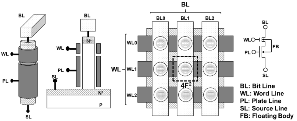
Fig. 6: The Unisantis cell. From left to right are a 3D view of the vertical transistor, a cross-section, a top view, and a schematic equivalent. Source: Unisantis
The word line still couples, but the charge it affects is only right at the end of the floating body. The charge within the PL region isn’t affected, so the coupling effect is greatly reduced.
Reading is non-destructive. Consequently, there’s no need to restore the contents after a read. Refresh is still required at the block level.

Fig. 7: The Unisantis cell (shown lying down rather than vertically) and the IV curve for the easier-to-read cell. Source: Unisantis
While this cell may be viable for a bulk stand-alone DRAM chip, that’s not the primary target at the moment. Instead, Unisantis is looking at L4/L5 cache that is embedded on an SoC. L1 and L2 (and likely L3) still need the speed of SRAM, but for the farther-away caches, density could be greatly improved with an embedded DRAM.
This cell uses no new materials, which helps adoption. In addition, the structure needs no charge pumps. “DRAM normally uses charge pumps for boosting word lines and a negative voltage in the substrate,” noted Sakui. “We don’t care about that.”
As a final surprise, this cell is technically non-volatile, so Unisantis is calling it dynamic flash memory, or DFM, to highlight both the DRAM and flash aspects of the technology.
Gain cells
The final cell style also gets rid of the explicit capacitor, aiming instead for gate capacitance as a storage location. The problem with standard silicon transistors, however, is they leak too much. That makes them impractical for memory.

Fig. 8: A gain cell as used by Georgia Tech and Imec. The transistors are thin-film oxide transistors. The unlabeled node at the bottom right is considered the read word line by Georgia Tech. Source: Imec
Instead, work at two different organizations is focused on oxides that can be used as conductors. “Oxide electronics has grown quite a bit,” said Raychowdhury. “There are oxides like vanadium dioxide, for example, where you apply a voltage or a current and it will heat up, and then there’ll be an electric field across it and it makes a phase transition.”
Work at Georgia Tech is replacing the two standard transistors in the cell with thin-film transistors made of indium oxide doped with tungsten, sometimes called IWO. This is a typical transistor used in displays, so it doesn’t represent a new material or device within the fabs.
“In the off state, it has a very large, wide bandgap, and you don’t have any conductance,” explained Raychowdhury. “You apply voltage, however, and the whole band structure comes up and down, and you allow electrons to flow.”
That stability makes it attractive for a 2T0C cell. There are two bit lines and two word lines, one each for read and write, so that has some area implication. And as a two-transistor cell, it’s not vertical. But it’s a stackable layer so that, again, area deficits can be overcome by layering.
How long data lasts on the node is a key consideration. “If you’re using it for a video buffer, where you have data coming in every millisecond, you probably do not need to refresh,” said Raychowdhury. “But if you are using it for cache, where you need the data to be resident for tens of seconds, then you would have to refresh.”
Because the memory cell is read through the read transistor channel, rather than the actual gate where the charge is stored, the read process itself is non-destructive. So refreshing after a read is not necessary.
Imec is working on a similar cell, but instead of IWO, it is using indium-gallium-zinc oxide, or IGZO, which also is used in displays. “IGZO, apart from the large band gap, also has some localized states next to the valence band, so it is possible to induce very, very low off currents by applying a negative gate voltage,” said Attilio Belmonte, senior scientist at Imec.
Imec claims to have achieved data persistence as high as 400 seconds. Again, it requires refresh, but less often.
The high data retention comes about as a result of lower leakage. While IWO leaks on the order of 10–15 A/µm, IGZO leaks at 10–19 A/µm, which is four orders of magnitude less. This low leakage is achieved using a negative voltage on the gate, but Imec is hoping eventually to eliminate the charge pumps. “Our final target will be not to use negative voltages,” said Belmonte.
Lower leakage allows for a smaller capacitance. IWO uses capacitors on the order of 1 fF, while IGZO can get by with a 38-aF capacitance.
One of the tradeoffs required is between leakage and read speed. Low leakage means negligible off current, but fast read speed means moderate — or even high — on current.
“It’s not a logic transistor, where you care about performance. Here, the focus is off current,” said Gouri Sankar Kar, program director at Imec. “IGZO solves the off-current purpose because it has a very high band gap, and it serves the on-current requirement because it has moderate mobility.”
Imec also is looking at how to build this structure using shared lithography for lower cost. Conceptually, the biggest difference between the Imec and Georgia Tech approaches is the thin-film material, so both approaches may be amenable to shared lithography. Imec didn’t go into any details on how that might work, however.
Georgia Tech and Imec don’t see this replacing bulk DRAM either, but rather acting as an L4/L5 cache embedded on an SoC. “If you look at commodity DRAM, the bit-cell size will be much smaller than this,” noted Raychowdhury. Imec also is looking at whether this can be used as an analog memory for in-memory computing.
Can new cells win?
Given the technical viability of a new bit cell, the next question is, can it displace the tried-and-true bit cell in use today? First of all, some of the technologies don’t even claim to replace DRAM. They’re targeting embedded applications that replace SRAM. Given success there, they may go on to do bigger and better things, but that involves much speculation.
The role of DRAM in systems may change as new memories create new options for the overall system memory architecture. “We have heard from sources in the industry that one of the options for the use of Optane (a cross-point non-volatile memory) was as a part of the DRAM area, so you basically have much less DRAM,” noted Ishai Naveh, CTO of Weebit. “And behind it, you have much more nonvolatile memory that is more or less as fast as DRAM on read, but slower on write.”
Chandrasekaran sees these architectural changes as giving standard DRAM more time to continue scaling. “Maybe there are other system solutions coming in place, such that the DRAM scaling cadence can have more time to continue planar a little longer,” he said.
Others are less convinced. “In my experience, none of the new approaches can really replace DRAM,” said Gary Bronner, senior vice president at Rambus Labs. “When people ask me, ‘What’s the future of DRAM,’ I tell them, ‘The future of DRAM is just DRAM.’ We know it’s going to get a little bit worse in terms of its reliability, and it’s going to be challenged for refresh time. Like a lot of other parts of computer systems these days, you’re going to solve that at the system level.”
That aside, there are two other main challenges — economics and inertia.
From an economic standpoint, stacking would need to allow a density bump so great that, even as it’s being released to the market, it already provides a cheaper alternative to standard DRAM. It’s likely to take 200 to 300 layers to do this, according to Chandrasekaran, limiting DRAM replacement only to those approaches using shared lithography.
The inertial barrier is not so easy to quantify. As with any mainstream technology whose demise is being foretold, practitioners of the traditional approaches tend to have lots of clever tricks up their sleeves to eke out yet more life from the current cell. Just as the end of CMOS has been forecast for decades, the end of DRAM has been in sight for years — and it’s constantly being pushed farther out.
“The DRAM industry makes huge numbers of DRAM,” said David. “They’re a $100 billion industry. So that translates into some gigantic number [of chips]. And so they are always learning.”
It’s entirely possible that there remain enough such approaches to keep the current cell alive for a long time. “While DRAM scaling has slowed, we are seeing a path where we can continue to drive the scaling for the next several years,” said Chandrasekaran.
That creates the challenge of shifting goalposts – unlike what happened with 3D NAND, where it was immediately evident when the change was needed.
“When the industry did 3D NAND, we could see the crossover,” said Chandrasekaran. “Planar DRAM keeps moving, and the crossover point keeps moving.”
Conclusion
It’s tough to know just how much benefit a new approach must provide in order to gain traction over the old approach. For all the excitement about innovation, companies usually prefer to innovate only as much as they really need to, and only if really needed. It costs money and a commitment to create something totally new.
It’s been estimated that it takes at least 10 years for any new bit cell to take hold. Some of these projects are already in year 3 or 4, but that suggests that it still will be years before we know how this story ends.
“While there are a lot of ideas, the research on monolithic 3D is still in the early phases,” said Aitken. “For now, HBM type stacking approaches with ‘classic’ DRAM are best. At some point in the future, that may change.”
Reference
[1] Sakui et al, “Dynamic Flash Memory with Dual Gate Surrounding Gate Transistor (SGT),” 2021 International Memory Workshop
Related
What’s Ahead For DRAM, NAND?
Semico’s CEO provides an outlook for the memory biz.
HBM Takes On A Much Bigger Role
High-bandwidth memory may be a significant gateway technology that allows the industry to make a controlled transition to true 3D design and assembly.
DRAM, 3D NAND Face New Challenges
Various memories and business outlooks are all over the map, sometimes literally, with lots of confusion ahead.
 |
|
 |
 |
 |  |
 |  |
Nicely done.