Scaling, packaging and a greater push for reliability add new challenges for testing chips.

It’s become increasingly difficult to manage the heat generated during IC test.
Absent the proper mitigations, it’s easy to generate so much heat that probe cards and chips literally can burn up. As a result, implementing temperature-management techniques is becoming a critical part of IC testing.
“We talk about systems, saying the system is good,” said Arun Krishnamoorthy, senior principal engineer at Intel, in a presentation at MEPTEC’s “Too Hot to Test” Conference. “But when it comes to the tester, we have problems. Test power can be 2 to 10 times that of the specified power.”
There are many ways to lower the temperature, but most of them increase test costs. The goal is to increase yields while protecting against escapes by managing both the tests and the temperatures in a way that minimizes costs. Still, some additional cost will pay for itself if it increases yields by even a little bit.
The issue isn’t limited to heat alone. Feedback loops can turn temperature issues into power supply issues, as currents increase and drive transient demands that supplies may not be able to keep up with. Voltage droop thus becomes a corollary problem.

Fig. 1: Heat and power issues ultimately arise from increases in power density over time. Source: Intel
This creates a challenge for test engineers and managers, who are typically last in the chain of tasks that must be completed for commercial production. The pressure is on, not only to finish the test programs, but also to ensure those tests are complete, that they protect the product, and that the solution meets cost constraints — meaning that test time is kept as short as possible.
Those requirements aren’t necessarily aligned, because some of the ways heat can be managed involve longer test times. If test strategies haven’t been worked out during the early device planning stages of the project, there may be unpleasant surprises as engineers figure out how to keep heat in check. This is becoming a critical consideration when testing large systems-on-chip (SoCs) and other large dies.
Test flows are different from system operation
Designers make careful choices to ensure that devices in operation don’t exceed the thermal design budget. But test insertion and vector generation traditionally don’t make those same choices. In fact, test circuits often bypass the power mitigations so that tests can be done more directly and efficiently. In addition, because tests can consist of quick bursts of intense activity, any thermal control loops in the chip may not have time to respond. That can allow the chip to overheat locally.
“With the system, we have thermal management, throttling, and power management, which keep the silicon within the power envelope,” explained Krishnamoorthy. “Scan test will kill all the thermal control loops because our test patterns are very short compared to the system benchmarks.”
Ultimately, this is an issue relating to the difference between how a device operates once soldered into a system and how test operates. Multi-core systems provide one clear example.
“For test efficiency, we usually run the cores in lockstep,” said Krishnamoorthy. “But it doesn’t happen on the system, because cores and threads are almost asynchronous, and the power is temporally distributed.” The resulting power is much greater than what normal operation would generate.

Fig. 2: The overall power profile of a chip as test progresses. Early in the cycle, initialization steps generate moderate heat. It’s the subsequent IP tests that have high bursts of activity, and the resulting hotspots move around the chip with different test sequences. Source: Intel
In addition, devices are assembled onto circuit boards in a manner designed to dissipate heat. “On the system, there is a robust thermal interface,” said Krishnamoorthy. “You put in a compliant or semi-permanent TIM [thermal interface material], with almost flat surfaces on the motherboard that has no warpage, and it’s screwed on properly.” In a tester, by contrast, contacts are optimized for repeated use with minimal wear, and the thermal mitigations that the in-system chip will enjoy won’t be in place.
So, not only may the chip be generating more heat, but it will also be less capable of dissipating that heat. That’s particularly the case for bare dies at wafer sort. “The bare die has low thermal mass,” Krishnamoorthy explained. “Its TJ [temperature at the silicon junction] rise is too fast for thermal handlers to respond to.” It’s even truer for singulated dies, since they don’t have the rest of the wafer to pull the heat away, and there’s likely material between the back of the die and any chuck.
Packaged parts, on the other hand, can fare better. “Lidded parts have a huge thermal mass, which has a very good thermal capacitance to reduce the transients,” Krishnamoorthy continued. “But thermal control equipment is too sluggish. Inside, the silicon the temperature is rising maybe in 10 milliseconds. By the time the thermal control equipment figures it out, it’s too late.”
In addition to the equipment responding slowly, a temperature rise may be noted too late. “Thermal mass is really a lagging indicator of what’s going on,” cautioned Ken Lanier, manager of Teradyne’s SoC Business Unit, in another MEPTEC presentation.
Thermally intensive tests are dominated by array tests, including memory built-in-self-test (MBiST) and repair operations; scan tests, particularly when run at speed; and other functional tests, including structure-based functional test and ported system tests, where snippets of code found to be problematic in-system are ported back into the test program.
Many of these tests are used not only on a pass/fail basis, but also for binning. Excessive heat can distort the performance of the chip at speed, potentially resulting in the throwing away of good dies or down-binning what could otherwise have been a higher-value die. Conversely, moving to a low-power mode may overstate speed and result in escapes.
If the heat becomes too intense at wafer sort, both dies and probe cards may end up burnt. No one wants to throw what might have been a good die away when it’s burnt.
“Particularly with AI functions and some high-performance chips, they require a lot of power,” said Alan Liao, director of product marketing at FormFactor. “So the current in the power map has doubled or tripled compared to previous chips. Can your probe sustain at that high current, or will it melt it down? At advanced nodes, the pitch is smaller and the drive in your probe is thinner. So you basically don’t have enough matter to take care of those currents.”
A damaged probe card for these devices can be expensive. “If a probe card goes away, then it’s easily $50,000 to $100,000. And there’s downtime for the line,” Krishnamoorthy said.

Fig. 3: Burnt probe cards and silicon as a result of excessive heat. Source: Intel
Heat can be tough to measure and control
Automatic temperature control (ATC) equipment is intended to help keep the chip within a suitable temperature range. It uses hot and cold liquid to move the temperature of the setup up or down as needed. The challenge lies in having the equipment respond fast enough. It’s a relatively long control loop between deciding that a die is too hot and seeing the temperature response of the ATC.

Fig. 4: Automatic Temperature Control equipment can help to cool excessive heat. Source: Advantest
“You do have a latency problem,” said Lanier. “By the time you monitor [the temperatures], get information to the ATC system, and the ATC system decides what to do about it, going through its own thermal delay, it’s a little late for what you need. The problem is that, while [these approaches] are adaptive, they’re not predictive.”
The first challenge is in determining the temperature. The package gives a lagging indicator. By the time it gets too hot, it’s likely too late for any temperature control to help the enclosed die.
A simple approach involves thermal diodes. “Anybody who’s doing this has multiple diodes around their device, and they switch to the various diodes on the fly,” noted Dave Armstrong, director of business development at Advantest, in his MEPTEC presentation.

Fig. 5: Power following is possible with power information available to be fed back, but it’s still a long control loop. Source: Advantest
One of the more promising approaches is to use on-die sensors or monitors in order to communicate any issues to the test setup for mitigation. The biggest barrier to this appears to be uniformity on how that data is to be made available. There are many sensors available, but they all communicate differently, making it hard to handle in a consistent fashion.
Lanier pointed to proteanTecs as a particularly promising monitoring setup. “The beauty of it is there is a controller on board, and that controller gives you a universal interface to the outside world,” he said.
proteanTecs is extending access to this interface. “Our UCT (Universal Chip Telemetry) architecture and analytics platform enable integration of third-party sensor data for a comprehensive monitoring solution,” noted Shai Eisen, vice president of product marketing at proteanTecs.
Given the appropriate correlations, this makes possible the ability to predict when temperatures are likely to rise before they’ve gone too far, providing extra time for ATC and other mitigations to have an effect. Those correlations must be established during initial characterization.
“It comes down to being able to accurately characterize the impact of the different environmental and functional mismatches across the different stages in the lifecycle of a chip, as manifested in wafer sort, final tests, system tests, and field functional performance,” said Eisen.
“We can correlate performance degradation to specific environmental or operational effects on the chip, like temperature surges or power supply issues,” added Eyal Fayneh, co-founder and silicon technologies senior principal engineer at proteanTecs.
The test programs also can send early indicators that a sequence known to generate heat will start soon, giving the ATC a head start. “It allows me to tell the thermal system to cool down early,” said Armstrong.

Fig. 6: Pre-triggering power can give the control loop a head start on cooling in anticipation of higher activity. Source: Advantest
If a tester is running tests on more than one chip at a time – so-called multi-site test – then this and other such mitigations must be done in a way that impacts one die without throwing another die off. That can be a particular challenge for dynamic testing flows, where each chip may experience a slightly different flow so that they’re not necessarily in lockstep.
Keeping power where it should be
The impact of sudden bursts of tests can go beyond things getting too hot. They also place a bigger burden on the power supplies than would be the case in-system. There may be multiple such power supplies, some dedicated to the different cores inside the chip.
“During scan testing, high-coverage test vectors can drive a substantial amount of on-die activity, often resulting in a significant power supply current draw,” said Dennis Ciplickas, vice president of advanced solutions at PDF Solutions. “This current draw can produce a large enough IR drop that an unintended toggle can occur and result in a scan test failure, a failure that would not be likely to occur during real-world usage.”
This sensitivity makes it critical that voltage sensing be as accurate as possible, which means measuring the voltage on the die at the core it’s powering. Measuring it any farther back toward the source can give inaccurate readings, making it harder for the supply to react as needed.

Fig. 7: Voltages should be sensed on-die for greatest accuracy. Source: Advantest
While power connections may run at the same voltage, it’s most effective to keep them on separate planes until they reach the die, merging them at that point. Otherwise, “If you have a contact problem, your current will flow through the contacts that are still there,” observed Advantest’s Armstrong. “You could have electromigration in addition to blowing up your part.”
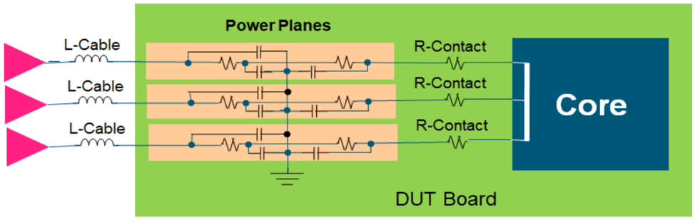
Fig. 8: It’s most effective to keep separate power signals on separate planes, merging only on-chip. Source: Advantest
The capacitors on the power lines are important, because at those times when the inductance limits the current, the capacitors step in. But the capacitance must be “just right” – something that test engineers must work on hand-in-hand with the tester vendor. “Too little is bad, too much can be worse,” observed Armstrong.
Bulk capacitors are used nearer the power source. Tantalum capacitors can work well here, because they can tolerate a wide temperature range — as long as you don’t expect negative power spikes. “Ceramic capacitors have some very nasty temperature problems,” said Armstrong. Since bulk caps are low-frequency filters, their lower high-frequency equivalent series resistance (ESR) isn’t an issue.
High-frequency caps also are needed near the device. High-quality ceramic caps work well here because of their low ESR.
How the power is engaged also can make a difference. “You don’t want to bring up all the supplies together from zero to one volt simultaneously, because you could have core-to-core shorts,” noted Armstrong. “You could also have one supply growing faster than the other, which could cause current flow from one core to the other that you don’t know about.” The best approach is to power up slowly and watch what happens, controlling the inrush current.
Fast-acting clamps also can help to protect against damage – and maybe even against thermal runaway. In a multi-site setup, if one clamp folds back, “you want to make sure you don’t fold back all the supplies for another site you’re testing,” noted Armstrong.

Fig. 9: Avoiding burnt dies and probes involves several steps, including inrush-current control, fast clamps, well-planned foldback, and final capacitor discharge. Source: Advantest
Attacking the source: DFT and the test program
Ultimately, it’s the tests that are at the root of the heat generation, given they don’t exercise the chip the same way that “mission mode” would. But mitigations must be traded off against test time.
“A different test sequence could be applied that reduces problematic and unrealistic chip activity and avoids potential IR drop or other signal integrity issues,” noted Ciplickas. “However, the tradeoff is usually an increased amount of time to run the test program, and more test time is not a commodity that product engineers typically have available.”

Fig. 10: Techniques for lowering test and operational power include minimizing voltage-domain crossings for scan chains, balancing low-power constraints against chain optimizations, and keeping test logic quiet during normal operation. Source: Synopsys
When running vectors, the scan-in and scan-out aren’t the problem, because they’re done at low frequency. “It’s the capture that is going to kill you, because this is one to two clock cycles,” said Krishnamoorthy. “And you are going to run at the top gigahertz.”
For instance, cores could be tested serially. For a four-core chip, that would quadruple the core-testing time with the benefit of keeping temperature down. A middle way might be to figure out the maximum number that can be reliably tested in parallel and to use as few passes as possible. The challenge is that there is at present no automated way to do this.
One can also reorder tests or insert patterns intended to cool the part (“narcoleptic” patterns) and distribute hotspots. Again, these are difficult to do manually, and there is no automation.
On-die monitors can help test development during new device bring-up. They can determine where in the distribution of performance an individual die lies. Correlating heat with vectors allows test developers to generate alternative vector series for different dies.
“By classifying a device’s material profile with unit-based granularity, you can select the best ATPG pattern sequence for that specific unit,” said Eisen. Such adaptive tests may run different dies through a different flow to keep heat in check. Where heat isn’t an issue, tests can be run more quickly to optimize test time.
Some DFT circuit improvements focus on reducing the number of signals toggling during different parts of the test operation. These include:

Fig. 11: So-called “Q-gating” can block scan data from exercising functional logic, reducing switching power. Source: Synopsys
Cron pointed to a situation that AMD was able to remedy. It had vectors running too quickly (100 MHz), generating too much heat and hurting yield. The “easy” solution was to slow the clock speed, but that would extend the length of the test. Instead, AMD slowed the clock to 62.5 MHz only for the most critical vectors. It then cranked the clock up to 125 MHz for the remainder of the vectors, making up for lost time and then some.
Other clocking mitigations can help, as well. “If you have a chip that has multiple shift clocks, you could misalign them so that the edges of the all the clocks don’t line up,” said Cron. “By the same token, you could misalign capture edges during shift.” If the test data is being delivered via a high-speed SerDes interface, then one has an opportunity to select different phases from the stepped-down clock in order to misalign edges.
Similarly, LBiST shifting can start slowly, ramping up to full speed before gradually slowing back down. The purpose of the ramping up and down is to give the power supply time to respond to the changing load.

Fig. 12: Ramping frequency up and down before and after LBIST helps the power supplies to keep up with the increased demand. Source: Synopsys
Lanier pointed in particular to the DFT scan bus announced by Siemens last year. It decouples many of the DFT moving parts from each other. “Now you can program how much data IP blocks are taking off the bus, how fast they’re taking it off, things like that,” he said. “So there are a lot of knobs here that disconnect what’s going on outside of the device from what’s going on inside.”
That involves keeping track of a lot of details. “It’s complex, but the fact that the scan data is so structured and that you have the exact same number of bits for thousands of patterns means you can leverage the advantage of the network doing that bookkeeping,” said Geir Eide, product marketing director for Tessent at Siemens EDA.

Fig. 13: Siemens’s Tessent scan bus decouples the data needs and rates of different IP blocks. Source: Siemens
Finding the right balance
Many of the opportunities to reduce excess test heat involve an equipment cost or longer tests. The question then becomes one of balancing the necessary improvements against those costs. And that comes down to an ROI calculation.
The best time to make that calculation is early in the design process. Involving test engineers at the early floor-planning stage can help identify which tests are going to be a challenge. The ROI for different solutions then can be evaluated early. If these considerations aren’t dealt with until a chip is overheating in a handler, then the range of possible solutions is much more limited.
Developing a test strategy while the architects and designers are developing their strategies will open up the biggest opportunities for reducing test heat without overly burdening the product cost. But in the end, it’s all about making the right tradeoffs.
“There is always a balance that must be made between overall test time for a device and subjecting a device to a sequence of tests that is so improbable that it results in unrealistic failures — or even worse, subjecting the device to stresses that could result in an early life failure,” said Ciplickas.
 |
 |
 |
 |
 |
 |
 |
The core issue is you are are trying to measure something that outside of mission mode. Power and temperature and not independent of function. You need to slow down test and replicate the applications thermal, and power integrity or what you observe isnt what the user will see. Besides burning them up, you are screening out otherwise good parts by subjecting them to out of spec conditions. I believe that the economics will favor in system distributed self-test so perhaps the single high cost tester bottleneck should ONLY focus on whether to package the bare die chiplet (with lower speed core functional tests) and a secondary more comprehensive speed, thermal and functional test set once in package with realistic environment rather than assume that can be approximated by a tester.