As logic devices become more complex, it took increasing amounts of time and effort to manually create and validate tests, it was too hard to determine test coverage, and the tests took too long to run. The technique is referred to as functional test. So the industry moved to a design for test (DFT) approach where the design was modified to make it easier to test. The approach that ended up dominating IC test is called structural, or “scan,” test because it involves scanning test patterns into internal circuits within the device under test (DUT). The design’s flip-flops are modified to allow them to function as stimulus and observation points, or “scan cells” during test, while performing their intended functional role during normal operation.
The modified flip-flops, or scan cells, allow the overall design to be viewed as many small segments of combinational logic that can be more easily tested. For a design with a million flops, introducing scan cells is like adding a million control and observation points. Segmenting the logic in this manner is what makes it feasible to automatically generate test patterns that can exercise the logic between the flops. The test software doesn’t need to understand the function of the logic-it just tries to exercise the logic segments observed by a scan cell. Since scan test modifies flip flops that are already in the design to enable them to also act as scan cells, the impact of the test circuitry is relatively small, typically adding about only 1-5% to the total gate count.
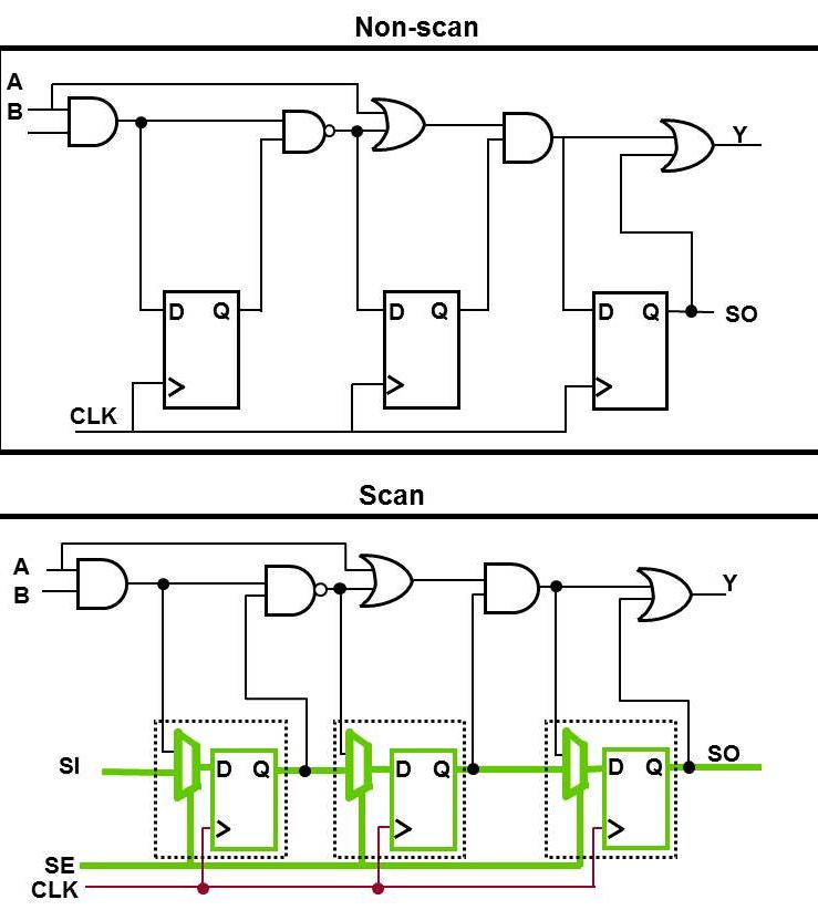
The scan cells are linked together into “scan chains” that operate like big shift registers when the circuit is put into test mode. The scan chains are used by external automatic test equipment (ATE) to deliver test pattern data from its memory into the device. After the test pattern is loaded, the design is placed back into functional mode and the test response is captured in one or more clock cycles. The design is again put in test mode and the captured test response is shifted out, while the next test pattern is simultaneously shifted in to the scan cells. The ATE then compares the captured test response with the expected response data stored in its memory. Any mismatches are likely defects and are logged for further evaluation.
Many designs do not connect up every register into a scan chain. This is called partial scan.
To enable automatic test pattern generation (ATPG) software to create the test patterns, fault models are defined that predict the expected behaviors (response) from the IC when defects are present. The ATPG tool then uses the fault models to determine the patterns required to detect those faults at all points in the circuit (or almost all-coverage of 95% or more is typical). There are a number of different fault models that are commonly used.
Stuck-At Test
The most basic and common is the “stuck-at” fault model, which checks each node location in the design for either stuck-at-1 or stuck-at-0 logic behavior. For example, if a NAND gate in the design had an input pin shorted to ground (logic value 0) by a defect, the stuck-at-0 test for that node would catch it. The stuck-at model can also detect other defect types like bridges between two nets or nodes. The stuck-at model is classified as a static model because it is a slow speed test and is not dependent on gate timing (rise and fall times and propagation delay).
At-Speed Test
A second common type of fault model is called the “transition” or “at-speed” fault model, and is a dynamic fault model, i.e., it detects problems with timing. It is similar to the stuck-at model in that there are two faults for every node location in the design, classified as slow-to-rise and slow-to-fall faults. The transition fault model uses a test pattern that creates a transition stimulus to change the logic value from either 0-to-1 or from 1-to-0. The time allowed for the transition is specified, so if the transition doesn’t happen, or happens outside the allotted time, a timing defect is presumed.
Path Delay Test
The “path delay” model is also dynamic and performs at-speed tests on targeted timing critical paths. While stuck-at and transition fault models usually address all the nodes in the design, the path delay model only tests the exact paths specified by the engineer, who runs static timing analysis to determine which are the most critical paths. These paths are specified to the ATPG tool for creating the path delay test patterns. The theory is that if the most critical timing paths can pass the tests, then all the other paths with longer slack times should have no timing problems. In a way, path delay testing is a form of process check (e.g., showing timing errors if a process variable strays too far), in addition to a test for manufacturing defects on individual devices.
IDDQ Test
The IDDQ test relies on measuring the supply current (Idd) in the quiescent state (when the circuit is not switching and inputs are held at static values). Test patterns are used to place the DUT in a variety of selected states. By performing current measurements at each of these static states, the presence of defects that draw excess current can be detected. The value of Iddq testing is that many types of faults can be detected with very few patterns. The drawback is the additional test time to perform the current measurements.
Toggle Test
Toggle fault testing ensures that a node can be driven to both a logical 0 and a logical 1 value, and indicates the extent of your control over circuit nodes. Because the toggle fault model is faster and requires less overhead to run than stuck-at fault testing, you can experiment with different circuit configurations and get a quick indication of how much control you have over your circuit nodes. Because the toggle fault model only excites fault sites and does not propagate the responses to capture points, it cannot be used for defect detection. This fault model is sometimes used for burn-in testing to cause high activity in the circuit.
N-Detect and Embedded Multiple Detect (EMD)
The basic idea of n-detect (or multi-detect) is to randomly target each fault multiple times. The way the fault is targeted is changed randomly, as is the fill (bits that don’t matter in terms of the fault being targeted) in the pattern set. This approach starts with a standard stuck-at or transition pattern set targeting each potential defect in the design. The pattern set is analyzed to see which potential defects are addressed by more than one pattern in the total pattern set. Then additional (different) patterns are generated to specifically target the defects that are detected a number of times that is less than the user specified minimum threshold. The combined information for all the resulting patterns increases the potential for detecting a bridge defect that might otherwise escape.
Embedded multiple detect (EMD) is a method of improving multiple detection of a pattern set without increasing the number of patterns within that pattern set. EMD uses the otherwise unspecified (fill or don’t care) bits of an ATPG pattern to test for nodes that have not reached their N-detect target. Standard multiple detect (N-detect) will have a cost of additional patterns but will also have a higher multiple detection rate than EMD. How much difference there is between EMD and multiple detect defect detection will depend on the particular design’s pattern set and the level of test compression used. This test is becoming more common since it does not increase the size of the test set, and can produce additional detection.
Deterministic Bridging
The deterministic bridging test utilizes a combination of layout extraction tools and ATPG. Based on a set of geometric rules, the extraction tool creates a list of net pairs that have the potential of bridging. This list is then fault simulated using existing stuck-at and transition patterns to determine which bridge defects can be detected. The net pairs that are not covered by the initial patterns are identified, and then used by the ATPG tool to generate a specific set of test patterns to completely validate that the remaining nets are not bridged.
Small-Delay Defects
At design nodes of 180nm and larger, the majority of manufacturing defects are caused by random particles that cause bridges or opens. There are very few timing related defects at these larger design nodes since manufacturing process variations cause relatively small parametric changes that would affect the design timing. However, at design nodes of 90nm and smaller, the same manufacturing process variations can cause on-chip parametric variations to be greater than 50%. This creates a situation where timing-related failures are a significant percentage of overall test failures.
One might expect that transition test patterns would find all of the timing defects in the design. This is true most of the time, but some of the smallest delay defects can evade the basic transition test pattern. For example, when a path through vias, gates, and interconnects has a minor resistive open or other parametric issue that causes a delay, the accumulative defect behavior may only be manifested by long paths. A common scenario is where the same via type is used multiple times in the same path, and the vias are formed as resistive vias. In order to detect this defect a small delay defect (SDD) test can be performed. Circuit timing and physical layout information is used to guide the test generator to detect faults through the longest paths in order to improve the ability to detect small delay detects. This ATPG method is often referred to as timing-aware ATPG and is growing in usage for designs that have tight timing margins and high quality requirements. The resulting patterns have a much higher probability of catching small-delay defects if they are present.
Page contents originally provided by Mentor Graphics Corp.
Recommended reading:
System-on-Chip Test Architectures: Nanometer Design for Testability (Systems on Silicon)