Imec’s An Steegen sees advanced packaging as a critical component of future scaling, including new bridge technology.

An Steegen, executive vice president of semiconductor technology and systems at Imec, sat down with Semiconductor Engineering to discuss IC scaling and chip packaging. Imec is working on next-generation transistors, but it is also developing several new technologies for IC packaging, such as a proprietary silicon bridge, a cooling technology and packaging modules. What follows are excerpts of that conversation.
SE: Chipmakers are shipping finFET transistors at 16nm/14nm with 10nm/7nm finFETs just beginning to ramp up. How far can we extend finFETs?
Steegen: The message is still the same. The companies will continue with the finFET as long as they find the performance boosters that meet the targets. Where we are since last year is that front- end gate transistor pitch scaling has been slowing down. It was already trending that way, but it definitely is slowing down. That typically buys you some time on the finFET to basically push it a little bit to the more advanced nodes. But today, with the relaxed front-end gate pitch scaling taken into account, we struggle to find the right performance boosters to basically make the targets for the 3nm type of generation.
SE: By performance or scaling boosters, you mean advanced modules to enable chip scaling. (These modules include self-aligned gate contacts and fully-aligned vias.) So what happens at 3nm?
Steegen: We are spending a lot of time, and the industry is spending a lot of time, still trying to come up with the performance boosters that can get us where we need to be with the finFET on 3nm. For instance, if we would find a breakthrough in low-k spacers, that would be a big help to treat the performance of the finFET. But today, it’s not at the values where it needs to be to make the 3nm targets. We are still working very hard on the high-mobility channel materials like silicon germanium and germanium. That will all buy you extra performance. So that’s happening. But on the other hand, we are also preparing the next device, which is a derivative of the finFET. That’s the nanosheet. It’s the nanosheet more so than the nanowire. The nanosheet is a little bit longer and wider. You have more performance when you go with a little bit wider nanosheet than a nanowire. It has better electrostatics. It opens up more of a performance window than a finFET.
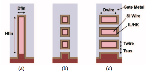
Fig. 1: Cross-section simulation of (a) finFET, (b) nanowire, and (c) nanosheet. Source: IBM
SE: When do we see the transition from the finFET to another transistor type, like the nanosheet FET?
Steegen: At 3nm for us today, the finFET is starting to struggle. So at 3nm, we need to find a serious performance booster for the finFET or we would have to make a change, let’s say to a nanosheet. For us, that’s 3nm. We count full nodes. We say 7nm, 5nm and 3nm. But let’s put it this way—it’s beyond 5nm.
SE: What is the timeline for that?
Steegen: If I have it right, 3nm is at the end of ’21 or early ’22.

Fig. 2: Next-gen transistor architectures. Source: Imec
SE: Today, customers can go down various paths. One way is to scale a device. Another way is to get the benefits of scaling by putting multiple devices in an advanced package. Some call this heterogeneous integration. This involves package types like 2.5D/3D, fan-out and system-in-package. Any thoughts?
Steegen: This is a path. So today, you already see some type of 3D heterogeneous integration in the package. You already have InFO (TSMC’s integrated fan-out) and EMIB (Intel’s Embedded Multi-die Interconnect Bridge). There are also some versions of wafer-level packaging going on in the industry. So, you can still have the best transistors on this 3D heterogeneous path. That will continue. It’s definitely a path not to ignore. This will happen and it will happen more and more.
SE: How do you see heterogeneous integration rolling out?
Steegen: There are, of course, high-performance systems. There are fan-out wafer-level packages. You can also go with a silicon bridge and through-silicon vias. Those provide power and performance gains. Cooling is a big thing and how to cool them. There is also mobile. In mobile, moving away from package-on-package to something more like fan-out wafer-level packaging will come.
SE: You brought up cooling. Imec recently introduced an impingement-based module for cooling chips at the package level. How is that used?
Steegen: This is for any of these high-performance packages. Even when you have a fan-out wafer-level package, you try not to put your memory on top of your processor. You still might have hot spots. Heat dissipation is quite difficult in these packages. You try to stagger your devices. Placing more micro-bumps and using the right materials also helps. It’s not enough. You need to cool the package. Today, there are cooling systems. If you have seen those, they are huge and very bulky. They are not necessarily very compact and also not close enough to the hot spot. What we designed is a very compact module. We can put it right there on the laminate on top of the backside of the hot spot. It’s very small.

Fig. 3: Imec’s cooling module technology; (a) schematic of multi-jet cooler; (b) Nozzle plate top view. Source: Imec
SE: Imec also is working on a stacking technology called sequential, or 3D monolithic integration. What is involved there?
Steegen: Sequential is still another technique. That’s where you build a second layer of devices on top of the first finished layer. In sequential, you develop your first layer even with the contacts or metal. You put the second layer on top and then you pattern it.
SE: In sequential, you have talked about stacking an analog device layer on top of the first layer based on logic. One application is smartphones. What is the benefit here?
Steegen: Today, in a modem, you take CMOS. And CMOS needs to have good analog performance. A finFET does not really help there. So what do you need to do there? You may need to have discretes in III-V. You want to pack them as close as possible. This lends itself to sequential. You can do III-V very close to the CMOS.
SE: What are some of the issues here?
Steegen: For 5G, we want to move to III-V devices. The question is, of course, how to get to these substrates. As you know, we’ve worked on this for a long time in logic. You have epitaxial growth. That’s still an option that you could still evaluate even for analog. The other one is that you pre-fabricate the wafer or the substrate on III-V. You layer transfer it on the CMOS.
SE: One of the big challenges with sequential or monolithic 3D technology is the thermal budget. You need to activate the dopants using the right annealing temperatures, but you also need to stay within a thermal budget, right?
Steegen: Everything is in material tuning today. Basically, you need to find different materials that can withstand different thermal budgets. Today, we are evaluating the performance of second layer and the first layer. So, we tune this with finFETs on finFETs, just to see that the devices don’t degrade. We’re within 10% for high performance devices. This means that we’ve tweaked the implants, anneals and the materials to such an extent that they are already within the range from meeting the target performance. You can optimize that.
SE: On the traditional packaging front, meanwhile, Imec is working on its own version of a silicon bridge technology for IC packages. How did that evolve?
Steegen: When we started this a long time ago. We called it a silicon interposer. Remember, it was actually quite big. It was a full silicon interposer, where you had the RDLs and the passives. Then, you put your logic and memory cubes on that. The point is, if your system becomes the SoC, it becomes bigger and bigger. That means if you want the silicon interposer underneath all of that, it becomes a very big chip, where you need to start thinking of stitching.
SE: To my understanding, Intel’s EMIB silicon bridge is embedded in the PCB. This connects the chips in the package. Imec’s silicon bridge is different. In simple terms, the assembly process takes place on a carrier wafer. Then, in the package, you put a small piece of silicon, or a silicon bridge, with vias at fine pitches. The bridge attaches one chip with another. How does Imec’s silicon bridge work?
Steegen: The silicon bridge, with this laminate package, is actually way more flexible. You have all of these building blocks now. You put in the laminate. Then, you only put the bridges, which are much shorter, between the blocks or dies that you want to connect.

Fig. 4: Imec’s silicon bridge vs. an interposer
SE: What are the apps?
Steegen: The electrical wires that we put in the silicon bridge have a very dense pitch. We are really driving the link speed. And what it does is connect memories to logic in your package. You also can think of other building blocks, of course. If you want to put an FPGA near your processor, that is also an example.
SE: Have you given up with 2.5D using an interposer?
Steegen: No. In the end, if you do it on a bridge or a silicon interposer, it’s the same concept. The only thing is how big do you want to make that silicon interposer. So maybe it’s a little bit more flexible to do it with a silicon bridge.
SE: In the past, you have talked about something called hybrid scaling. What is that about?
Steegen: There are two names for it. Some say heterogeneous integration. Others say hybridization. In principle, we mean the same thing. What that actually means is you have a system that you want to partition into blocks. You want to use the preferred IC technology for that block, and then you find a way to package that altogether in the most compact way.
SE: Are you still pursuing that?
Steegen: Of course. Actually, in our logic, memory and interconnect programs, they now work together. It involves what we call STCO, or system-technology co-optimization. You can do many things with that. We are working on what we call integration boosters for STCO. For instance, you can have a backside power distribution network. If we can take that away from the front side, you improve area and power. You can put that somewhere in the package at the backside of the wafer. You gain area and power.
SE: This is like what you are doing with transistor scaling. You are developing scaling boosters. The difference is that you are developing boosters for the package, right?
Steegen: It’s just like what we do for scaling boosters in design technology co-optimization or DTCO. This involves technologies like self-aligned gate contacts. Now, at the system level, you can start at the SoC level, also with the intent on doing that. That is definitely coming.
SE: So what happens to traditional IC scaling?
Steegen: So when you say: ‘Do you continue scaling?’ The answer is yes. We continue with power, performance, area, cost scaling at the SoC level. That means the transistor level. That means the circuit level. But it also means the systems level. That’s the layers of the onion. You must work on all of them together.
Related Stories
Choosing The Right Interconnect
Toward High-End Fan-Outs
Fan-Out Wars Begin
Cheaper Packaging Options Ahead
 |
 |
 |
 |
 |
 |
 |
Leave a Reply