Next-gen etch methodology is necessary and mature enough, but it’s still slow.

The semiconductor industry is developing the next wave of applications for atomic layer etch (ALE), hoping to get a foothold in some new and emerging markets.
ALE, a next-generation etch technology that removes materials at the atomic scale, is one of several tools used to process advanced devices in a fab. ALE moved into production for select applications around 2016, although the technology is still not widely deployed because it’s a slow process. Now the industry is looking at new applications for ALE in memory and logic, as well for III-V materials and exotic metals. ALE stands a chance to crack these and other markets, providing it can overcome some challenges.
ALE is one of several types of etch technologies in the market. Etch itself works in conjunction with deposition. In chip production, a chipmaker deposits a material on a wafer using a deposition system. Then they use an etch system to remove the unwanted materials using a chemical process. The mainstream etch tool type is called reactive-ion etching (RIE), which has been used in chip production for decades. Basically, an RIE-based etch system removes materials in devices on a continuous basis.
At advanced nodes, RIE etchers and other equipment are used to manufacture chips, although there are some challenges. As the chip dimensions become smaller at each node, chipmakers are processing mere atoms during the flow. So in select steps in the fab, chipmakers use equipment that processes chips at the atomic level, namely atomic layer deposition (ALD) and ALE. ALD, which is a mature technology, deposits films at the atomic scale.
ALE is newer and less mature. Generally, vendors offer standalone ALE equipment or integrate these processes within their RIE-based etchers. Using a two-step process, ALE selectively removes targeted materials at the atomic scale without damaging other parts of the structure. “With ALE, you’re isolating the different steps,” explained Rick Gottscho, CTO of Lam Research. “By separating things in time and space, now you’ve broken the problem down into smaller pieces, each of which can be optimized independently.”

Fig. 1: Schematic of ALE process based on sequential surface modification and volatile release reactions. Source: University of Colorado
Unlike RIE etch tools, ALE isn’t used for every device in the fab. “ALE has its applications in certain ways in places like memory and things like that. But it’s not widely used where you need to do it everywhere,” said Risto Puhakka, president of VLSI Research. “The market size for ALE compared to the overall etch market is still fairly limited. Developing a new technology takes time.”
ALE won’t solve every problem in the fab, although it is considered a valuable tool in the toolbox. So in R&D, there is a flurry of activity around ALE. At the recent ALD/ALE 2020 conference, companies, R&D organizations and universities presented papers on what’s next in ALE. They include:
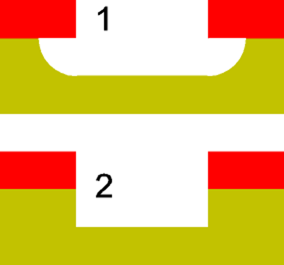
Fig. 2: Isotropic or unidirectional etch (top) vs. anisotropic or directional etch (bottom) Source: Wikipedia
What is etch?
Despite the difficult business climate, the semiconductor equipment market is expected to reach $82.7 billion in 2020, up 7.3% over 2019, according to VLSI Research. “Business is strong,” said Dan Hutcheson, CEO of VLSI Research. “It’s being driven heavily by China. The growth in China for the equipment industry is offsetting any kind of weakness anywhere else.”
Of that figure, the etch market is expected to reach about $12 billion in 2020, up 8% over 2019, according to VLSI Research. In 2021, the etch market will grow by 6%.
Based on market share, the “Big 3” etch suppliers are Applied Materials, Lam Research and TEL, according to the firm. AMEC, Hitachi High-Tech, KLA and others also compete in the market.
Within the overall etch market, ALE is still small, representing a “few hundred million dollar” business, according to VLSI Research. Applied, Lam and TEL are the major ALE players. Hitachi, Oxford and others compete here.
Etch isn’t new. The technology can be traced back to the late 1960s, when Signetics conducted the early work in plasma etch. Then, in the 1970s and 1980s, several commercial etch vendors emerged. In the 1980s, universities began to explore ALE.
On the technology front, the etch market is split into two categories—wet and dry. Wet etch uses liquid chemicals to remove materials. Dry or plasma etch, the larger of the two markets, involves ALE and RIE.
In fabs, the workhorse etch tools are based on RIE technology. In an RIE etch system, a wafer sits in a reactor with a plasma source. Gas is introduced into the system and the plasma breaks up the gas, generating ions and reactive neutral species. Then, the ions and species bombard a pre-defined part of the wafer, which removes the materials.
Years ago, the processes were simple. An RIE etcher would simply need to etch a trench or other structure in a single material.

Fig. 3: Simplified illustration of dry etching process. Source: Wikipedia
Today’s logic and memory devices are more complex, which presents some challenges for etch and other equipment. Take 3D NAND for example. Unlike planar NAND, which are 2D structures, 3D NAND resembles a vertical skyscraper in which horizontal layers of memory cells are stacked and then connected using tiny vertical channels.
3D NAND is quantified by the number of layers stacked in a device. As more layers are added, the bit density increases. Today, suppliers are shipping 96-layer 3D NAND devices with 128-layer products in the works.
“3D NAND flash memory has enabled a new generation of non-volatile solid-state storage useful in nearly every electronic device imaginable,” said Timothy Yang, a software applications engineer at Coventor, a Lam Research Company. “3D NAND can achieve data densities exceeding those of 2D NAND structures, even when fabricated on later generation technology nodes.”
But in 3D NAND there are several deposition and etch challenges. First, vendors deposit alternating thin films on the substrate. The process is repeated several times until a given device has the desired number of layers. Then, using an RIE etcher, tiny channels are drilled from the top of the device stack to the substrate. The aspect ratios are 50:1 for 96-layer devices.
Each tiny channel must be parallel and uniform, which is a challenging task. “You not only have to control the CDs and overlay, but also address challenges associated with profile control for these new and very tall device structures,” said Efi Megged, director of product marketing at KLA.
Besides 3D NAND, advanced transistors, DRAM and the new memory types also have complex structures with different materials.
To deal with these challenges, chipmakers require advanced RIE etchers. These tools must handle a multitude of processes. A chipmaker tunes the etcher for each process.
“An etcher has about 300 sensors. You have power. You have chemistry and flow rates. You have so many different parameters to what controls that etcher,” said Ben Rathsack, vice president and deputy general manager for TEL America, in a recent presentation. “You are using different chemistries. You’re going after certain etch profiles, especially for high-aspect ratio etching. That’s becoming extremely critical.”
Moving to ALE
Besides RIE etchers, chipmakers also use ALE for advanced chip production. Today’s advanced chips consist of three parts—transistors, contacts and interconnects. The transistor serves as a switch.
The interconnects, which are on top of the transistor, consist of tiny copper wiring schemes that transfer electrical signals from one transistor to another. Then, a layer called the middle-of-line connects the transistor and interconnect pieces using tiny contact structures.
At each node, the transistor structures are becoming smaller and more complex. “We are getting down to small dimensions at this point,” said Robert Clark, senior member of the technical staff at TEL, in a presentation at the ALD/ALE 2020 conference. “We’re approaching the point where we need to start counting the atoms.”
This in turn presents some deposition and etch challenges. “The structures are becoming taller and thinner. We need to operate around curves and underneath where we can’t even see what we’re trying to deposit on,” Clark said.
There are some solutions. “The way to do that is to bring in what I call self-aligned technologies. We need self-aligned structures that enable us to land, for instance, a via from one metal level to another level,” he said. “We need atomic-scale technologies like atomic layer deposition (ALD) and atomic layer etching (ALE) in order to control the thicknesses of high-aspect ratio structures with good conformality.”
ALD is used to deposit materials on a surface, one monolayer at a time. It’s a slow but dependable process. For years, chipmakers have used ALD in logic and memory.
ALE, which also is slow, is the opposite of ALD. Using a two-step, self-limiting process, ALE removes materials. In some cases, ALD and ALE could work together in the same process.
After years of R&D, ALE finally moved into production around 2016. Initially, the technology was used for self-aligned contacts in chips. It has expanded into other areas.
Consider contacts, for example, which are structures with tiny gaps. ALE is used to form those gaps, which subsequently are filled with cobalt. The process involves pumping a reactant on the surface, then using a second reactant to remove the materials and form the gap. The trick with ALE is to do this without damaging other parts of the structure.
In one example of ALE from Lam, a wafer resides in a chamber in an ALE system. The first step is to inject chlorine gas on a silicon surface in the chamber. The chlorine molecules are absorbed on the surface, which in turn modifies the surface. Then, argon ions are injected in the chamber, which bombards the surface and removes the modified layer, according to Lam.
“With ALE, you take that modified layer and you put in some source of energy and you desorb it selectively,” Lam’s Gottscho said. “You can do that with ions, or you can do it with temperature, or you can do it with photons. You’re cleaving the bonds between the underlying layer and the modified substrate. Those bonds are weaker than the bonds within the substrate itself, which is why you get ‘one layer’ removed at a time. That’s in quotes because it’s typically more than one layer because the surface modification wasn’t one layer. It has some depth to it.”
There are two types of ALE—plasma and thermal. Plasma ALE, which is in production, enables directional or anisotropic etches. “Plasma ALE removes surface species with energetic ions or neutral atoms. Because of the directionality of the energetic ions and neutral atoms, plasma ALE yields anisotropic etching that is needed to fabricate high-aspect ratio features,” said Steven George, a professor of chemistry at the University of Colorado (CU).
Thermal ALE, which is more challenging, uses thermal reactions for unidirectional or isotropic etches. Today, plasma ALE is making inroads, while thermal is still the development stages. “I do not believe that thermal ALE is in production,” George said. “However, many vendors are working on thermal ALE.”
Both ALE types are ideal for certain applications. For example, ALE can be used to remove materials in a structure to form trenches with gaps on the order of 10 to 15 angstroms, or 5 atoms wide. (An angstrom is 0.1nm.)
In another application, plasma ALE can be used to process contacts. ALE also is used as a smoothing technique to fix the line-edge roughness issues caused by EUV patterning.
In many applications, ALE isn’t required or is too slow. Traditional RIE can do the job. The decision to use one technology over another depends on the application, cost and performance.
Nonetheless, the industry continues to develop plasma ALE. One metric for ALE is what Lam calls “synergy.” The term describes how much of ALE is generated minus the unwanted reactions. The goal is to obtain a 100% synergy in an ALE process.
In silicon-based processes, plasma ALE works. At times, though, silicon-based ALE processes are prone to unwanted reactions. The synergies are sometimes in the 80% to 90% range, according to experts.
As it turns out, plasma ALE obtains higher synergies in what Lam calls “super-ALE” materials, which are generally resistant to heat and wear. Diamond, amorphous carbon and various refractory metals are considered “super-ALE” materials. GaN is also promising.
“What do they all have in common? They all have high surface binding energy,” said Keren Kanarik, senior technical director at Lam, during a presentation at the ALD/ALE conference. “Take a material that is tough and hard to etch. And that’s what you want for ALE. It’s about strength that makes the material also resistant to those bad reactions.”
This in turn opens the door for a new class of materials that can be used with ALE. For example, ALE could help smooth out surfaces for “super-ALE” materials. In another application, Leti and Lam recently presented a paper on using plasma ALE for gate-etch applications in GaN. “The strategy chosen for gate patterning is the recess gate, meaning a deep recess (more than 100nm) into the stack to produce a normally-off transistor. ALE processes are very promising because they permit a GaN etching with few degradations, but they are very slow. Therefore, an etch with full-ALE processes is not suitable for industrial environment due to the etch duration,” said Simon Ruel, a researcher at Leti. “The solution developed was to start the gate etching with classic, fast plasma process and finish by a few ALE cycles. This combination provides faster etch rates and reduction of degradation.”
More ALE
Thermal ALE, meanwhile, is also an active area for research. Unlike plasma ALE, which is making inroads, thermal ALE is just taking root. “Thermal ALE is still in its infancy,” CU’s George said. “There are still many more materials to demonstrate by thermal ALE. Understanding the mechanisms of all the various pathways for thermal ALE is still in development.”
The industry is just beginning to understand these mechanisms. “The main thermal ALE mechanism for metal oxides is based on fluorination and ligand-exchange reactions,” George said in a recent paper. “Fluorination is the surface modification reaction. Fluorination is thermochemically favorable because most metal fluorides are more stable than their corresponding metal oxides. One difficulty with fluorination is that some metal fluorides are volatile. These metal oxides require a different thermal ALE mechanism.”
Nonetheless, researchers are exploring several applications for thermal ALE. They include:
Thermal ALE also will be important for “deposit and etch-back” strategies using a combination of ALD and ALE. “ALD will be used to deposit a continuous film, and thermal ALE will be used to etch back the desired thickness. The ‘deposit and etch-back’ strategies will be important for ultra-thin films that cannot be formed directly using ALD because of nucleation difficulties,” George said.
Today, some but not all of these applications use traditional RIE, which is proven and cost-effective. Thermal ALE will require some new breakthroughs to crack these markets.
But if the industry can advance thermal ALE, the technology has some advantages. Thermal ALE is less prone to damage. And as devices become more 3D, isotropic etches are needed. Using a skyscraper analogy, RIE can etch the vertical elevator shafts but not the horizontal hallways.
With that in mind, the industry is targeting isotropic ALE for next-generation nanosheet FET transistors at 3nm and/or 2nm. A nanosheet FET is a finFET on its side with a gate wrapped around it.
In a simple process flow, a nanosheet FET starts with the formation of a super-lattice structure on a substrate. This structure consists of alternating layers of silicon-germanium (SiGe) and silicon on the substrate.
Then, vertical fins are formed in the super-lattice structure, followed by the development of inner spacers. In this step, the outer portions of the SiGe layers in the super-lattice structure are recessed using an isotropic etch technique. This is an extremely difficult process.
However, IBM and TEL recently described a etch technique for this application. This involves a horizontal isotropic SiGe dry etch technique with a 150:1 aspect ratio.
Meanwhile, at ALD/ALE 2020, the University of Delaware presented a paper on the use of thermal ALE for metals and alloys, namely cobalt, iron and CoFeB (cobalt-iron-boron). CoFeB is of interest because it is used to form the magnetic tunnel junction (MTJ) stack in a next-generation memory technology called STT-MRAM.
“The nature of these materials is such that one of the chemical steps in their ALE has to be controlled kinetically to achieve a true ALE regime, which we have shown by combining surface chlorination and reactions of chlorinated surfaces with diketones,” said Andrew Teplyakov, a professor at the University of Delaware. “However, in order for the processing conditions to be selected for combined alloyed metals, the mechanism of the etching has to be understood.”
Recently, researchers have uncovered the basic reasoning behind the mechanisms here. “For the applications including MTJ, ALE is promising because it’s an effective and precise method to remove the material, and because the process does not increase (and actually decreases) surface roughness,” Teplyakov said.
Also at the conference, CU presented a paper on thermal ALE for a tantalum-oxide (Ta2O5) compound and tantalum-nitride (TaN). The goal is to use Ta2O5 and TaN for metal gates. Ta2O5 is a useful dielectric material.
Still, thermal ALE for metals is challenging. “Selectivity is challenging because metal precursors are needed that will produce stable and volatile products of one material during ligand-exchange,” CU’s George said. “However, similar ligand-exchange reactions are not desired for other surrounding materials. Knowledge of which metal precursors will produce the desired stable and volatile products by ligand-exchange reactions require a broad understanding of chemistry.”
Conclusion
ALE is definitely a technology to watch. It could help enable next-generation logic and memory chips, not to mention other technologies.
Based on the challenges with these and other chips, chipmakers need all the help they can get.
Related Stories
Challenges In Stacking, Shrinking And Inspecting Next-Gen Chips
 |
|
 |
|
 |
 |
 | |
 |
 |
#/media/File:Etch_anisotropy.png)
#/media/File:Photolithography_etching_process.svg)
Leave a Reply