
Success at the edge takes advantage of common threads — lithography, imaging, chiplets, and AI.

Key Takeaways:
With a healthy boost from AI and high-performance compute, medical devices, electric vehicles, and humanoid robots enabled by semiconductor technology today are poised to transform lifestyles tomorrow. To accomplish this goal, engineers are leveraging commonalities across disparate applications to achieve economies of scale across many industries and make chiplet commercialization feasible.
As portability efforts increase, companies are taking co-development among partners to new levels to surmount the challenges of sub-2nm. Nowhere is this more important than in advanced lithography.
Increasing die size drives reticle stitching solutions
With considerable engineering effort, existing tools often can be used to address entirely new problems. For instance, the lithography exposure field is limited by the reticle size (26 x 33 mm). That limits the size of modern chips, which is especially important for SoCs. The solution to date has been to divide functionality among chiplets, breaking down the SoC into smaller chip sizes.
A competing approach is to stitch two adjacent fields together by running patterns across the edge of the reticle, forming one chip across both fields. “There’s a lot of technical complexities with stitching, because you’re now introducing these borders between patterns on your chip. The field edge introduces significant distortion, which affects imaging,” explains Germain Fenger, senior director of product management at Synopsys. “Normally, we ignored this because it’s at the edge of the die, but now the edge has made it to the middle, so part of this involves modifying the design to optimize routing placement across the fields.”
Leading chipmakers already use inverse lithography technology (ILT) and optical proximity correction (OPC) at the most critical exposure layers at 5nm and beyond. ILT is a computationally intensive process, with long write times, that produces curved features on the mask. This process accounts for the distortions introduced by the optics and process variations, resulting in straight lines on the wafer.
“We also may modify design rules locally, if they need to be modified,” said Fenger. “Basically, it’s a combination of OPC and ILT that enables the best lithographic performance, and at imec we can validate our tools for this difficult patterning challenge. Imec is also the perfect environment to think outside the box to see not just how we can do more of the same, but maybe do something different in the flow to solve this challenge.”
Automotive through vertical integration
One of the most significant trends in the automotive industry is the shift from older-node chips to leading-edge processes, particularly for ADAS and autonomous capabilities.
“The semiconductors used in a vehicle are very, very diverse,” said Vidya Rajagopalan, senior vice president of electrical hardware at Rivian. “We have high-performance application processors, we have real-time processors that are very reliant on being jitter-free, we have cellular modems, we have RF performance, we have GNSS, and we have electromechanical products, mechatronic products, displays, audio, speakers.”
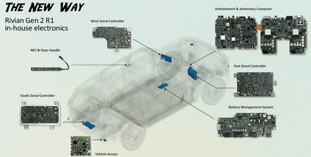
Fig. 1: Vertical integration simplified the electronics to just a handful of PCBs. Source: Rivian
Rivian’s first-generation in-house autonomy processor, RAP1, is a custom 5nm SOC from TSMC that is integrated with three HBM stacks. Interestingly, the company is able to use virtually the same hardware platform, broken into three to five zonal PCBs for all its vehicles, trucks, and delivery vans. “By 2030, about 50% of the car’s bill of materials will be electronics, which also reflects the growing software complexity that comes with the modern vehicle.”
Rivian took a vertically integrated approach to EV design, simplifying the electronic content. “Until recently, most OEMs acted as integrators of units purchased from Tier One suppliers, and the Tier One suppliers all specialized in different things,” Rajagopalan said. “As a result, the vehicle contained 40 to 100 electronic control units. We had the luxury of looking at this as a clean sheet of paper, so we see our vehicle as one large network computer. We design nearly all the electronics, which is much simpler. Only two companies in the western hemisphere have done this, along with a bunch of companies in China.”
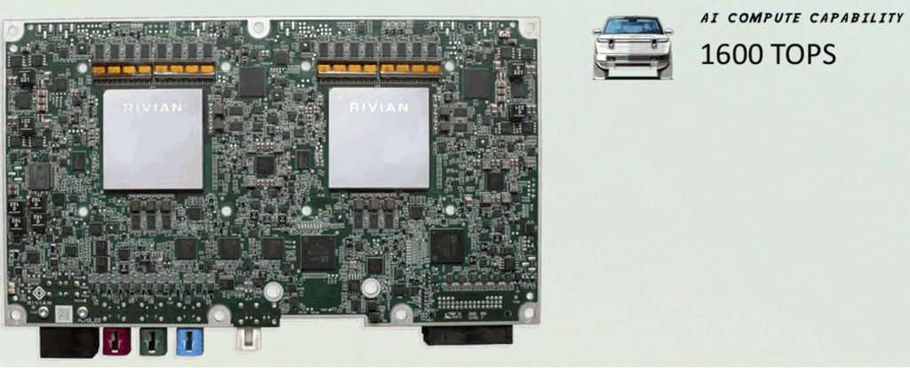
Fig. 2: Under the hood of the MCMs sit leading-node SoCs surrounded by HBMs. Source: Rivian
That will likely change. “You’re going to see far more sophisticated packages in automotive, much more complicated multichip modules — memory, SoCs, and power management,” she said. “A lot of people talk about determinism and low latency in physical AI, but we assume these in a self-driving car.” The company’s third-generation technology and vehicles are due out later this year.
Using co-development, but kicking it up a notch
Co-development is not a new concept in the industry, but it’s being taken to new levels to meet the stringent performance specifications of sub-5nm devices and chiplet-based packaging. “At advanced nodes, performance is no longer driven by single steps, but by the interaction between processes such as bonding, thinning, CMP, and packaging,” said Douglas Guerrero, senior technologist at Brewer Science. “Together with imec and its partners, materials can be tested across full process flows rather than isolated steps, improving robustness.”
For example, one imec collaboration with Brewer’s scientists resulted in a commercial-ready material platform that meets tighter performance specifications for thermal stability, adhesion, and ultraclean debond with reduced process variability, all of which enabled faster adoption in manufacturing. “Without imec, the project likely would have taken longer due to limited access to integrated process flows and cross-industry feedback loops.”
One base technology, dozens of applications
Several examples show how base technologies can be adapted to multiple uses, such as optical filters deposited on CMOS image sensors that enable hyperspectral imaging. Hyperspectral imaging can help preserve healthy tissue during surgery, ensure the freshness of food, optimize water use in crop fields, detect blood or gunpowder at crime scenes, or separate plastics for automated recycling, among several other uses.
Hyperspectral imaging captures the signature of materials from close-up, as in identifying layers in antique oil paintings. From great distances, compact cameras can be fitted on drones for everything from warfare to determining exactly which crops need watering.
This imaging technology is built on commercial CMOS image sensors. “The filter is made up of a lot of flat thin layers that make the transmission peaks, so they have spectral responses we design them for. By choosing different materials and different thicknesses, we can simulate what the total transmission will be,” explained Tina Babu Shylaja, R&D engineer at imec. Many filters can be integrated and aligned with lithographic precision to individual pixels with a pitch of ~5 μm. A wet cavity etch creates a staircase over the pixel array, allowing each step to act as an independent optical filter while the thickness of the transparent cavity determines the central wavelength of the filter.
Breakthrough medical devices
imec researchers are developing a variety of medical devices designed to replace more risky techniques already in use. “We are focusing our research on using neuromodulation implants to address chronic problems like essential tremor or depression,” said Milind Pandit, an imec R&D engineer. “We focus on vagus nerve stimulation or deep brain stimulation using ultrasound. The reason we use ultrasound rather than electrical stimulation with probes is that ultrasound is a bit more versatile in steering waves to specific points in the brain. That is important because research on the brain is still up and coming, which means people are not completely aware of the mechanisms and the areas of stimulation that lead to certain results. Furthermore, scar tissue doesn’t form, because you’re not actually penetrating the brain tissue. It is only from the surface of the structure, so somatosensory problems due to the waves reflecting back from the skull do not come into play.”
One hyperspectral imaging application that has received FDA clearance in the U.S. is used for open and minimally invasive surgical applications. “The surgeon wants to remove all the unhealthy region, while sparing as much healthy tissue as possible,” said Josh Gibson, head of technology at Hypervision Surgical. “Crucially, you need to cut where there is still sufficient blood flow, then stitch it back together so that you have blood flow across that joint for good healing.”
The hyperspectral camera detects oxygen saturation levels in tissue and may help identify tissue at risk from ischemia. That allows for maximum preservation of healthy tissue.
Yet another exciting area is hyperspectral imaging of the retina of the eye to provide early-stage diagnosis of signatures for brain conditions, including Alzheimer’s, Parkinson’s, and Huntington’s diseases. Because these typically are diagnosed after onset, the idea of this imaging is to have a non-invasive method of identifying the signature associated with each disease before symptoms appear.
Interestingly, using AI in medicine can mean a variety of breakthroughs even without introducing any new technologies or instruments. “It’s pretty extraordinary that most measurements in health undergo some form of wave-forming compression, and because of that compression, we are often losing the medically relevant data that we want based on either human perception or human values that we want to collapse that data into,” said Dan Wattendorf, director of Accelerator Global Health at the Gates Foundation. “When we look at the initial ML and transformer-based AI learning models just on the waveforms of an EKG, we’re starting to see astonishing things that no clinician or cardiologist can see. Embedded in that data, you can see whether someone had atrial fibrillation a decade ago. We can see structural heart defects that are only seen on ultrasound in the EKG signal.”
Wattendorf explained that compression of data is even more dramatic in a CBC (complete blood count) reading where 9 million data points are compressed to about 20 numbers viewed by the physician. In tracking 12,000 healthy patients over a 20-year period, Mass General Brigham Hospital showed that individuals whose data fall within specification levels can have very different distributions and setpoints, resulting in no detection of strong variance outside of one’s baseline. “This is clear to any data scientist, but we need to have access to that data. We haven’t even begun to look at the uncompressed data behind these medical waveforms.”
Humanoid robots
There is an argument for reusing some technology even in something as new as humanoid robots. “In talking to developers of humanoid robots, they emphasize they cannot afford to rewrite the compute stack for each of their robots. Determinism, openness, and scalability are the driving forces behind physical AI architectures, not peak TOPS,” said Salil Raje, senior vice president and general manager of AMD’s adaptive and embedded computing group. “Such a system has a brain that is doing the perception, planning, and decision-making, and it’s running large language models. The spine in the middle is a synchronous fabric that connects up most of the nodes. This is typically run on time-sensitive networks. It has one global clock, and it aligns all the nodes to within microsecond latencies. And then you have the body — hundreds of sensors that are fusing data from vision, from audio, from motors, with forces and inertia data. The limb controllers are doing the slacks and safety moves, and then you have the joint and the motor controls doing the torque and actuation.”
To meet latency requirements, Raje said that meeting real-time response requires data to be maintained locally. “You encode the data, you filter the data, you resize the data, and you send only insights, tokens, metadata to the central brain, and that enables a two to three orders of magnitude of improvement in data traffic.”
Efficiency and reliability rule in physical AI
Sensing data is critical in physical AI, but it needs to be energy-efficient. “We can leverage bio-inspired technologies for edge AI to improve efficiency,” said Ahmed Bahai, chief technology officer at Texas Instruments. “For instance, our brains are processing data in a very different way, a much more efficient way than current devices. In fact, you can debate whether its capacity is 1016 FLOPs (floating point operations per second), or 1015, but that doesn’t matter. What matters is that the efficiency of our brains is about 10,000 times greater than anything we have produced today. And it does not use an LLM, but an SLM (sensory language model). Even a baby learns languages from a few words and then uses intuition to build their vocabulary. So there is a lot we can learn when power is at stake, because today’s devices are more power-limited than transistor-limited.”
This core focus on energy efficiency will be a must for generative AI and physical AI acceptance, especially among the general population.
Progress from automotive informs everything autonomous
At its International Technology Forum (ITF), imec announced that it renamed the Autonomous Edge Chiplet Program (AECP), which builds on the foundational expertise and technology approaches of the Automotive Chiplet Program (ACP), launched in 2024. To date, the ACP has assembled 24 members, including OEMs, Tier 1 suppliers, IC manufacturers, EDA companies, and OSATs. A separate program helped catalyze CHASSIS (Chiplet-based Hardware Architectures for Software-defined Vehicles), which grew out of the ACP as a joint European project led by Bosch.
“We just opened our new site in Heilbronn in Germany, a chiplet acceleration center that is designed to bridge the gap between research and industrialization. The center has one goal — to really focus on prototyping — driving compliance and making sure that we’re de-risking prioritization of chiplets for the automotive industry,” said Dieter Hoffend, director of business development for AECP.
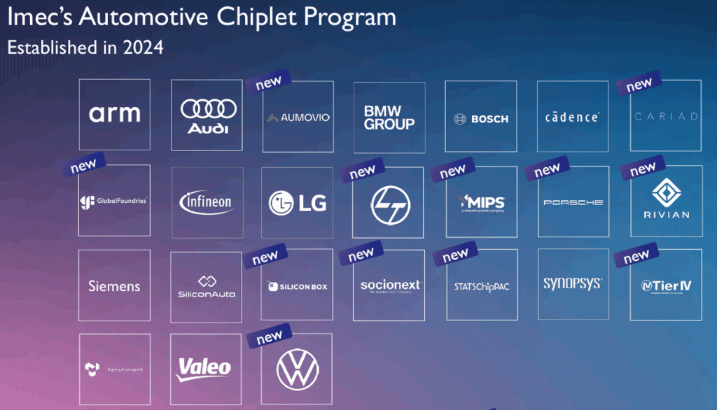
Fig. 3: The ACP is global, bringing together OEMs, Tier 1 suppliers, semiconductor manufacturers, EDA firms and OSATs. Source: imec
Portability from the CHASSIS hardware/software reference platform to similar platforms is another goal. “There is a common architectural DNA within chiplets that scales across multiple industries,” said Hoffend. “It has to do with compute, AI, safety, memory, and scalability. All of the same kinds of challenges that we are addressing in the ACP apply to the AECP. What differs is certainly the specifications associated with those vertical segments, and as such you may see different I/Os, different sensing applications, etc. But we truly believe that the core of what we do in automotive will be scalable into other segments. Reusing architectures will reduce the cost and accelerate time to market.”
Hoffend emphasized how important this shared expertise is. While 96.4 million vehicles were manufactured in 2025, volumes for individual vehicles remain fairly flat from year to year compared to those found in consumer electronics. “Automotive is a relatively small market from a semiconductor perspective. So how do we reconcile exponential compute demand with linear market economies? We at imec believe chiplets are the answer.”

Fig. 4: The chiplet-based reference design for physical AI will take foundational learning from the ACP and form an architectural foundation for humanoid robots, drones, and industrial automation. Source: imec
The group has set a 12-month deadline to build a reference platform for edge applications, prioritizing interoperability among chiplets from multiple vendors and hardware/software co-design. He added that the Automotive Chiplet Program is not confined to EU member states, and that imec is working with Japan’s Advanced SoC Research for Automotive (ASRA) to harmonize the standardization of chiplet architectures for automotive applications. The organizations have agreed to jointly explore and promote shared architecture specifications.
Conclusion
For all the disruption, it’s important to remember that much of the progress made on the technology front is being layered atop existing platforms, methods, and techniques that have worked in the past. That includes co-development agreements between companies such as imec, Fraunhofer Institute, and CEA-Leti, along with suppliers, chipmakers, and end customers.
Large challenges — like making stitching work across reticle fields, or making chiplet platforms compatible with products from different vendors — will require the closest of partnerships and collaborative thinking. Multiple solutions will be needed, and no single company can solve the challenges of sub-2nm processing and advanced packaging alone.
Related Articles
AI Data Centers And Auto Industry Converge On Same Issues
The EV revolution relies on battery innovation, while AI data centers need a range of new energy solutions to play nice with the grid. Both sectors are taking notes.
AI-Defined Vehicles Increase Pressure On Auto Ethernet Reliability
Time-sensitive networking and MACsec allow Auto Ethernet to handle safety-critical functions and enable real-time processing for AI-enabled features and agents.
Humanoid Touch And Voice Are Improving Rapidly
General-purpose humanoid robots need all their senses to function equally well; vision and movement are the farthest along, but others are catching up.

 |
 |
 |
 |
 |
 |
 |  |
 |  |
 |
 |


Leave a Reply