Enabling mask and process engineers to explore new patterning methodologies and assess alternate scenarios.

Producing modern semiconductor devices is an immensely challenging process. Successful execution entails advanced process nodes, novel device architectures, new materials, and many fabrication steps. One especially challenging area is lithography, in which light is sent through a photomask, passes through a projection system of lenses and mirrors, and strikes the substrate to create the device structures. In the early days of chip production, this light was at the edge of the human-visible spectrum, produced first by mercury lamps (l = 365nm).
Today, the lithography process is far more complex. To further shrink and pattern the smallest features of a chip, exposure tools use light of shorter wavelengths, in the deep ultraviolet (DUV) region of the spectrum, generated by excimer lasers (l = 248nm or 193nm). The features on the photomask are becoming of similar dimension as the exposure wavelength, pushing the imaging process to its physical limits.
For the fabrication of the most advanced semiconductor devices, chip makers have switched to lithography systems using an even shorter wavelength, impacting the entire patterning flow, including photomask technology, photoresist material systems, and metrology. High-power pulsed lasers create a plasma from molten tin droplets, which delivers light in the extreme ultraviolet (EUV) region of the spectrum (l = 13.5nm). Due to the short wavelength, the projection system of the exposure tool is built based on mirrors, and so is the photomask, as shown in Figure 1.
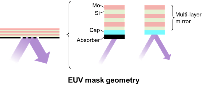
Fig. 1: Photomask technology for EUV lithography.
An EUV mask consists of a reflecting mirror made up of multiple layers of molybdenum and silicon. The patterned absorber film prevents incoming light from being reflected, thus generating the corresponding image on wafer level. In both cases, phase effects of the exposure light are used to enhance contrast and image quality.
Physical fabrication takes too much time at too high a cost to be the primary method for developing and optimizing lithographic patterning options. Instead, the entire lithography process—from light source to mask to imaging to pattern formation in the photoresist—can be simulated to a high degree of accuracy and predictability. This enables mask and process engineers to explore new patterning methodologies and assess “what if” scenarios without the cost of experimenting in silicon. Of course, test chips are still produced, but only after the simulations have narrowed down promising new approaches.
Simulating the entire lithographic process based on physical models is complex and time consuming, given the large parameter space and the growing area of critical layout clips. Each step within the lithography process flow is represented by dedicated simulation components, each of which uses multiple subroutines and solvers to describe the propagation of light, i.e., electro-magnetic waves, in the optical system, or the reaction kinetics of material species within the photoresist system.
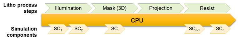
Fig. 2: Simulation flow on conventional CPU hardware.
Figure 2 illustrates the simulation flow for a standard lithographic process, from light source through mask and projection system to the formation of a 3D resist profile on wafer level. Traditionally, simulations are executed on CPU-based (central processing unit) high-performance compute systems. While the clock speed, and therefore the compute speed, of a conventional CPU entered a saturation phase during the past few years, multi-core CPUs and multi-CPU systems offer the opportunity to further reduce the overall turn-around-time (TAT) by using parallel processing of simulation steps, either through multi-threading or distributed processing. However, the scaling of TAT, i.e., simulation time, reduction with increasing numbers of CPU cores depends strongly on the problem description, leading to a saturation of performance gain.
Looking at alternative hardware solutions, graphics processing units (GPUs) moved into the focus, as those chips had been designed to further accelerate compute-intensive algorithms and solvers. Although originally developed for applications such as computer gaming, GPUs have proven valuable in many domains. They offer a high degree of parallelism, with thousands of cores rather than dozens.
The time spent within the individual steps of the lithography process simulation flow very much depends on the complexity of the computation. The same is true for the TAT benefit a GPU-based computation offers over a conventional CPU. One of the most time-consuming steps in the flow is the precise treatment of the mask, where the small dimensions of features demand a computation of the electro-magnetic field propagation through the absorber and the multi-layer, rather than using simple geometric optics.
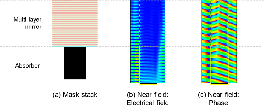
Fig. 3: EMF simulation results of the mask, showing near field intensity and phase effects that will impact imaging performance in resist, on the wafer.
The electro-magnetic field distribution within the mask is determined by solving Maxwell’s equations, resulting in specific information about the intensity and the phase of the individual field components, as shown in Figure 3. This very compute-expensive step can consume more than 90% of simulation time of the entire flow.
Recent tests have shown the high value of GPUs for lithographic simulation of real-world chip designs. We ran these test cases using the Synopsys S-Litho predictive lithography simulation solution, which deploys physics-based models to enable high simulation accuracy and predict the outcome of a photolithographic process. To take advantage of GPU acceleration within S-Litho, we are transitioning individual solvers step by step to GPU. In the first phase, solvers are tuned for CPU multi-threading before optimizing them for GPU support.
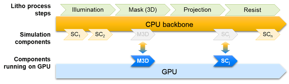
Fig. 4: Simulation flow on CPU+GPU hardware.
With the Mask3D simulation step being one of the most time-consuming in the flow, we started the move to GPUs with both S-Litho Maxwell solvers, the FDTD solver (finite difference time domain solver) and the WaveGuide solver (a derivative of an RCWA solver, rigorous coupled wave analysis solver), considering individual optimization steps for DUV and for EUV light, as well as Manhattan, all-angle polygons, and curvilinear geometries. Other simulation components have followed or will follow, as shown in Figure 4.
The main part of the simulation flow, the simulation “backbone,” continues to run on CPUs. It handles the GUI, data input and output, the distribution of independent tasks on CPU workers, as well as the data transfer between CPU and GPU systems to achieve a maximum degree of parallelization. At the same time, the data flow between CPUs and GPUs is optimized to reduce overhead time.
The GPU acceleration of the Mask3D component significantly reduces the overall simulation runtime, enabling applications that were impractical due to excessively long runtimes on CPU-only hardware.
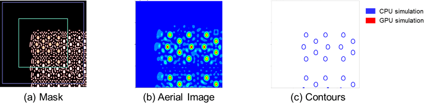
Fig. 5: GPU performance test case on EUV Mask3D.
Figure 5 shows an example resembling the corner area of a memory array. The mask layout (a) covers a simulation area of about 1 x 1 µm² and shows main as well as assist features. The aerial image intensity is shown in (b) and the resulting resist contours are shown in (c), where both CPU and CPU+GPU results are compared. Within the numerical resolution limits of the simulation, the results are identical, i.e., the acceleration is achieved without impacting simulation accuracy.
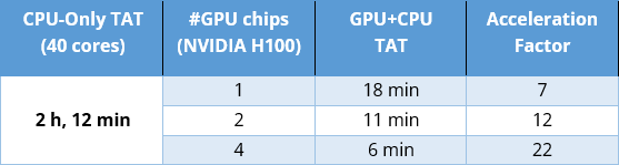
Table 1: GPU runtime overview.
Table 1 shows the runtime results for the testcase illustrated in Figure 5. While this testcase takes more than two hours on a CPU with 40 cores, without an option for further CPU-based acceleration, the deployment of GPUs reduces TAT to minutes. Moreover, performance scales well with the number of available GPU chips on the host.
The acceleration factors strongly depend on the simulation setup, the type of solvers used within the flow, the memory size of the problem to be solved, and the CPU/GPU parallelization scheme. For another testcase, we analyzed the GPU acceleration of the Mask3D solver and compared it to the speedup of the entire simulation flow, which includes resist pattern formation.
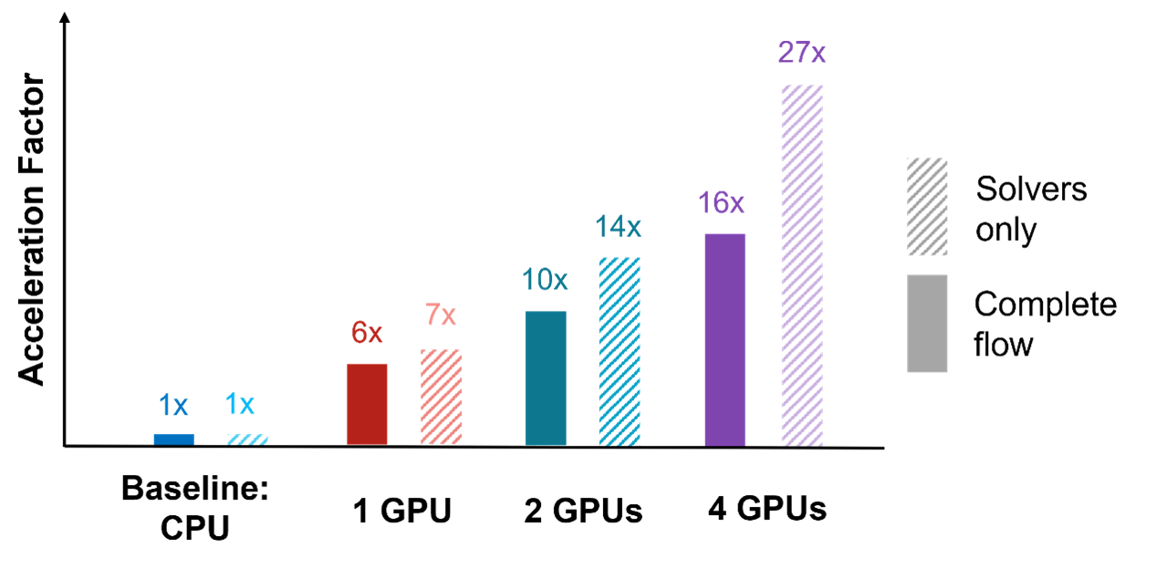
Fig. 6: Scaling of simulation time with the number of NVIDIA H100 chips.
Figure 6 summarizes the performance of our GPU solvers by analyzing the speedup achieved through GPU acceleration. Both the speedup of the solvers themselves (algorithm and data transfer) and the overall speedup of the complete simulation were investigated. To evaluate the solver’s scalability, we conducted experiments using varying numbers of NVIDIA H100 GPUs. The baseline CPU simulation was performed on a 32-core system.
S-Litho on GPU achieves excellent scalability without compromising result accuracy. These significant speedups not only benefit our users but also enable them to explore new research fields. For instance, the observed runtime reduction now enables the direct use of rigorous models within correction (rigorous Synopsys Proteus OPC) or verification (rigorous Synopsys Proteus LRC), which could result in a significantly improved resist 3D aware correction or 3D hotspot detection on cell level.
 |
|
 |
|
 |
 |
 | |
 |
 |
Leave a Reply