Spotting defects with existing inspection tools is getting harder, but upgrading to new technology is expensive.

The current defect inspection systems for packaging are running out of steam for the latest advanced packages, prompting the need for new tools in the market.
In response, several vendors are rolling out new defect inspection systems for use in various advanced packages, such as 2.5D/3D technologies and fan-out. The new defect inspection systems are more capable than the previous tools, but they are also more expensive. And packaging houses may need to buy different types of tools.
All of this comes at a time when the industry is trying to reduce the overall cost of advanced packaging. For years, the industry has used various inspection equipment to locate defects in IC packages. Existing defect inspection systems are suitable for commodity packages as well as the current advanced package types in the market, such as 2.5D/3D technologies, fan-out and others.
But the latest advanced packages are migrating towards finer features with more layers and I/Os. As a result, the defects are becoming smaller, making them harder to find using the current inspection systems. The inability to detect defects has a direct impact on yields for a given device.
“In many cases, the core inspection technologies that worked for the large dimensions, like the first-generation eWLB, are now running out of gas, and new inspection technologies are being deployed,” said Stephen Hiebert, senior director of marketing at KLA-Tencor. “You used to have macro inspection (for IC packaging). Now, these tools for advanced packaging have to find micron and sub-micron level defects.”
For example, embedded wafer-level ball-grid array (eWLB) is one of various fan-out packages in the market. Generally, fan-out is measured by the line and space features in the redistribution layers (RDLs) within the package. An RDL consists of copper metal connection lines that are routed in the package. Line and space refer to the width of the metal traces and the space between them.

Fig. 1: Redistribution layers (RDLs) are used to reroute connections to desired locations. Source: Lam Research
As more complex chips are integrated into a fan-out package, it may require more RDL layers with finer lines and spaces. For example, today’s fan-out packages range from 5µm line and space (5-5µm) and above with 2-2µm and below in the works.
“As companies go to the next technology nodes, the bump pitch becomes finer and inspection capabilities will have to improve,” said Jan Vardaman, president of TechSearch International. “As features (lines and spaces) shrink to 2µm and below, it becomes more difficult to see defects. In addition, finding debris in via holes becomes a concern in some applications.”
All told, the industry needs new defect inspection systems for the latest advanced packages. These capabilities are critical in several applications like automotive, where there is a zero-defect policy. Other markets require these capabilities as well.
Seeking to address the challenges, KLA-Tencor, Rudolph and others recently introduced new optical-based defect inspection equipment for advanced packaging, which addresses RDLs at 5µm and below. In addition, vendors have introduced new infrared inspection tools for the die sort production phase.
Packaging trends
For years, the emphasis in the IC market has revolved around traditional chip scaling, cramming more functions on a device and then shrinking it at each process node. The package was an afterthought and simply housed the device.
Recently, though, chip scaling has become more expensive and complex at each node. Today only a select few can afford to design chips at advanced nodes. For example, IC design costs alone have jumped from $51.3 million for a 28nm planar device to $297.8 million for a 7nm chip, according to IBS.
This is not to say that chipmakers have stopped scaling. But advanced nodes are not required for analog, RF and other chip technologies, which are growing at a fast pace. “We do anticipate steady growth in automotive and specialty technologies such as power management, RF and embedded non-volatile memory,” said Steven Liu, senior vice president of marketing at UMC.
Advanced packaging is part of the mix. Starting just after the turn of the millennium, the industry began to look for alternatives to chip scaling, namely advanced packaging. Instead of scaling the features on a monolithic die, the idea behind advanced packaging is to integrate dies in the vertical direction.
Advanced packaging has been used in limited form for decades in niche applications. The issue is cost as the technology remains too expensive for many applications.
Still, advanced packaging continues to make progress as the industry moves towards a concept called heterogeneous integration. “The key area where we need to contribute in assembly and test is in heterogeneous integration,” said David McCann, vice president of packaging R&D and operations at GlobalFoundries. “This is where you package multiple chips from a node or several nodes, or even bring in several suppliers into an integrated package level.”
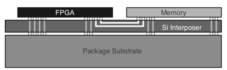
In one example of this trend, the industry has been shipping 2.5D technology. In 2.5D, dies are stacked on top of an interposer, which incorporates through-silicon vias (TSVs). The interposer acts as the bridge between the chips and a board, which provides more I/Os and bandwidth.

Fig. 2: FPGA + HBM in 2.5D package with interposer. Source: Xilinx
“2.5D enables an order of magnitude increase in interconnect density. What you are trying to address is memory bandwidth and latency. That’s the purpose of the interposer with very fine line and space,” McCann said.
GlobalFoundries, for one, has been shipping 2.5D/3D technologies with TSVs at 5µm (diameter) x 55µm (depth). It is qualifying TSVs at 2µm x 20µm.
Other packages are moving towards finer features, namely fan-out. In fan-out, the dies are packaged while they are still on the wafer.

Fig. 3: Fan-Out WLP Source: Lam Research
Introduced more than a decade ago, fan-out originally had RDLs with large dimensions and few I/Os. In comparison, today’s high-density fan-out has more than 500 I/Os and less than 8μm line/space. TSMC’s InFO technology, the most notable example of fan-out, is incorporated in Apple’s latest iPhones.
“Today, we are seeing an order of magnitude level of scaling,” KLA-Tencor’s Hiebert said. “We are seeing 2μm RDLs in production and there are RDLs of 1μm or below in development.”
Some fan-out packages have three or four layers of RDLs. “The industry is trying to move to more RDL layers, finer pitch RDL layers and larger packages. If you have fan-out or multi-die fan-out, the footprint is going to be bigger. As the package scales, and as the number of layers increase and the RDL shrinks, all of these creates substantial yield challenges. And finding and controlling defects is critical,” Hiebert said.
That’s where defect inspection fits in. “As we go to finer line and space, it’s fair to say the challenges are getting pretty significant,” said Eelco Bergman, director of sales and business development at ASE.
“As you move to finer RDLs, particularly to multi-layer RDLs, how are you going to check the quality for that? You need some mechanism of monitoring your inline performance to help drive your process optimization and to get your yields as high as possible. And for other cases, you might need at least some post-fabrication validation capability,” Bergman said.
That’s just for fan-out. 2.5D/3D packages have other challenges. And there are other types of packaging that are under development, such as chiplets, that could result in new packaging approaches.
Chiplets are more of a LEGO-block type of approach, connecting various pre-developed hard IP blocks together using an interconnect fabric. DARPA is spearheading a push in this direction to reduce costs and time to market, and a number of companies are exploring similar options, including Intel, eSilicon and Qualcomm.
“The goal is to take all of the functionality of a chip on a smaller die and add in flexibility,” said Amin Shokrollahi, CEO of Kandou Bus. “You can distribute different parts of a neural network on chiplets, but for flexibility the die placement is really important and the spaces have to be very short.”
How these chiplet packages ultimately will look isn’t clear, and neither are the inspection challenges. Still, the general trend is the same as with other types of packaging—shrinking distances and overall area to improve performance and reduce power and area.
The role of inspection
To find defects, packaging houses use defect inspection, metrology tools and failure analysis systems. Inspection is the art of finding defects in products, and it is used in both the fab and packaging house. This is not to be confused with metrology, which measures and characterizes structures in devices.
Fabs and packaging houses use different inspection systems, although both entities are striving to achieve similar goals—they want to find and eliminate killer defects in devices, thereby boosting yields in the flow.
In the fab, chips are measured at the nanoscale and the defects are sometimes at the angstrom level. For this chipmakers use expensive e-beam and optical wafer inspection systems.
In packaging, the defect sizes are larger and measured at the micron or sub-micron level. Packaging houses use tools based on optical, infrared and other techniques.
Generally, the inspection requirements are different in the fab and packaging. “Although the evolution of advanced packaging processes may appear to be simply the migration of front-end technologies to back-end operations, packaging processes create structures and use materials that are not typically found in the front-end,” said Tim Kryman, senior director of corporate marketing at Rudolph Technologies. “As a result, they have unique inspection and measurement requirements that cannot be met by existing front-end tools.”
For the most part, inspection has been relatively inexpensive for packaging, but that’s changing in some segments. “One challenge for these suppliers is the changing economic paradigm,” Kryman said. “Packaging has traditionally been regarded as low-tech and low-cost. Low prices and margins have exerted relentless pressure to keep operating and capital costs to a bare minimum. Advanced packaging processes are now requiring investments in equipment and technology that traditionally were found in front-end fabs.”
Finding defects
In the traditional inline packaging flow, packaging houses use high-speed, optical-based defect inspection systems. Camtek, KLA-Tencor, Rudolph and others sell systems in this market.
The older inspection tools work for most package types and will continue to be used for many years, but it’s a different story for the latest 2.5D/3D and fan-out technologies.
Typically, an inspection tool can find defects at one-third to one-half of the critical dimension. At one time, for example, a packaging house was developing a package with 10μm RDLs. For this, they would use an inspection system that could detect defects at around 3μm and above.
But that’s not good enough for the latest packages, which have RDLs at 5μm and below. So for this, a vendor needs an inspection tool that can find defects sizes at 2.5μm and smaller, even sub-µm defects.
“The processes are getting more complicated. Hence, there is more inline monitoring using inspection and metrology data. And you use that to ramp yield up from R&D to high-volume production levels,” KLA-Tencor’s Hiebert said. “Many of the inspection technologies that were able to run at 10μm or 20μm RDLs are really challenged to go to the 1μm or below level.”
This includes the latest fan-out packages. In fan-out, the chips are first processed on a wafer in the fab. Then the chips are diced and placed in a wafer-like format based on an epoxy mold compound.
Then a multi-layer RDL stack is created on top. To make the RDLs, a copper seed layer is deposited on a surface. After that, the desired RDL structures are patterned and developed.
At this point, the structure undergoes a defect inspection step. If there is a defect issue, the packaging house can fix the problem by re-working the wafer.
Then, once that step is completed, the remaining RDL steps are conducted. This process is repeated for each RDL layer.
After the package has been produced, it undergoes a final defect inspection step. In total, a fan-out package with three or four RDL layers may require between 10 and 15 inline inspection steps.
But even with all of these steps, it is still challenging to find all defects. “There are numerous defect challenges for advanced packaging applications,” said Amandine Pizzagalli, an analyst at Yole Développement.
Seung Wook (S.W.) Yoon, director of group technology strategy for the JCET Group, noted there are at least three major defect challenges for today’s advanced packages. “First, tiny or thin foreign materials/residues can surface at the bottom of a small via in a dielectric layer. Second, thin metal bridges at metal lines and spaces (trench structures) surface when the space is narrow and metal line is high (high aspect ratio). And third, multi-layer RDL inspection is challenging for finer line widths and line spacing with foreign matter present,” he said.
This, in turn, is driving the need for better inspection. “Like the front-end, shrinking feature sizes are driving the inspection requirements for improvements in accuracy, precision, sensitivity and throughput,” Rudolph’s Kryman said. “RDL line geometries are already below 10µm and are continuing to shrink with defect sensitivity running at roughly 50% of the printed line and space dimensions. Bump size, pitch and height continue to decrease as well. Manufacturers also are challenged by the diversity of packaging processes and rapidly changing requirements.”
Some of those requirements are the result of the packaging itself, which is the impetus behind a variety of new approaches currently under development to limit problems such as warpage, which itself can cause defects. In effect, this is addressing the problem several steps ahead of the actual packaging.
“One option is to use a thin film pre-bond where you lay a chip inside a stencil in the mold compound,” said Rama Puligadda, executive director of advanced technologies R&D at Brewer Science. “The result is that you don’t have warpage, which is a growing problem with EMC (epoxy mold compound). You also can take a more modular approach to reduce warpage.”
Regardless, inspection needs to discern new and complex patterns. “The metal patterning for applications such as fan-out tend to be highly complex. Compared to front-end applications, we see much more irregular shapes. We see diagonal lines. We see other structures that aren’t electrical in nature. We see structures that are for thermal or structural reasons that are inserted in the metal layer,” KLA-Tencor’s Hiebert said.
Meanwhile, responding to these and other challenges, KLA-Tencor, Rudolph and others have introduced new optical defect inspection tools, which are geared for RDLs at 5μm and beyond.
The latest systems from vendors use both brightfield and darkfield techniques. In brightfield imaging, light points directly above a sample. The light hits the sample and the system collects scattered light from the object. In darkfield imaging, the light hits the sample from an angle. In both cases, the data is analyzed for defects.
Each vendor also offers different features on their systems. KLA-Tencor’s new Kronos 1080 system is designed to inspect advanced wafer-level packaging process steps. It provides flexible substrate handling, which supports bonded, thinned, warped and diced substrates. The tool uses a technology called FlexPoint, which focuses the system on key areas within the die. This is where the defects would have the highest impact.
Meanwhile, like its predecessor, Rudolph’s new Dragonfly G2 platform combines 2D and 3D inspection and metrology capabilities in a single platform. But it has higher throughput and sensitivity. It can detect defects as small as 1µm. In addition, it adds a technology for detecting non-visual defects.
More inspection
After this process, the package moves to final test and assembly, sometimes called die sort. The packages are diced and then inspected in this process.
Several problems can surface here. The low-k materials used in today’s devices are fragile. During dicing or other steps, cracks can surface on the sidewalls of a fan-out package, as well as memory packages and bare dies.
“These materials are more subject to cracking and breaking during the dicing process,” said Pieter Vandewalle, general manager for the ICOS division at KLA-Tencor. “Some new defects arise like these dicing cracks, which require new types of inspection.”
For this application, KLA-Tencor has entered the die sort inspection market with a system based on infrared techniques. KLA-Tencor’s new ICOS F160 system performs inspection and die sorting. The tool also enables six-sided optical inspection capabilities.
Meanwhile, Mühlbauer and other vendors also compete in the die sort inspection space.
The path forward
New inspection tools are arriving as the industry is ramping up next-generation packages. These systems hope to address the yield/defect issues.
Still, the industry must address cost. Generally, advanced packaging is still too expensive for many OEMs. Apple and a few others are the exceptions to the rule.
That must change. Traditional chip scaling is becoming prohibitively expensive and many OEMs are taking a harder look at advanced packaging. The question is whether packaging houses can meet the cost and yield challenges for the next wave of technologies.
 |
|
 |
|
 |
 |
 | |
 |
 |