Complex interactions and tighter tolerances can impact performance, power and life expectancy.

Variation is becoming a much bigger and more complex problem for chipmakers as they push to the next process nodes or into increasingly dense advanced packages, raising concerns about the functionality and reliability of individual devices, and even entire systems.
In the past, almost all concerns about variation focused on the manufacturing process. What printed on a piece of silicon didn’t necessarily match what was supposed to be printed. But increasingly, other types of variation are playing a role. It is becoming much more difficult to predict, detect, and prevent issues for a growing number of reasons. Among them:
While variation of any type in one particular spot is probably manageable using existing tools and processes, variation in multiple places is much more difficult to deal with. It’s harder to pinpoint, and more complex to resolve.
“As the processes and features they create become smaller and more complex, manufacturers face an increasing need for high-precision inspection and measurement to detect defects and improve process control,” said Tim Skunes, vice president of R&D at CyberOptics, noting the problem is even more complex in advanced packages. “Bump height is fundamentally three-dimensional, and bump height is just as important as the size and location. Controlling bump height, both absolute and relative to neighboring bumps (co-planarity), is critical to ensuring reliable connections between stacked components. Processes use expensive known good die, making the cost of failure extremely high, driving the need for 100% metrology and inspection. If one bump fails, the whole package fails.”
Some of this is uncharted territory for the chip industry. “The big problem is overall system variation,” said Andy Heinig, group leader for advanced system integration and department head for efficient electronics at Fraunhofer IIS’ Engineering of Adaptive Systems Division. “There are methods available to compensate for variation, but we’re also encountering new problems that were not known up until now.”
Understanding variation effects becomes particularly difficult to manage inside a package if everything isn’t visible. This is made worse by the fact that many of these devices use customized layouts. Current leakage through a gate oxide with one or two fewer atoms may or may not have a significant impact on another component, depending upon the floor plan. And it’s made still worse by the fact that many of these designs are manufactured in relatively small batches, so there is less time and historical perspective to correct issues.
“As you get more die inside of a package, the problems are compounded,” said Ken Molitor, COO of Quik-Pak. “Some of our customers are putting, for example, resistors and capacitors inside of their package so they can trim the R’s and C’s later to compensate for some of the offsets. They’re trimming to meet the specification of the multi-chip module, trying to take some of that variation from die-to-die out of the picture.”
Placement plays an important role here. “Sometimes variation from die to die is too much, and you can’t accurately dial in the necessary offset,” said Molitor. “Then you have to start over, or replace one of the die. It gets complicated. We deal with engineers on a one-on-one basis to work through these things. What we’re seeing is a lot of time is now being spent making single-die silicon that we want to package to match the designer’s simulations more accurately.”
That’s one piece of the variation picture. “Two other variation trends worth mentioning, independent of the advanced packaging process used, are variation in pre-package bare die, as well as the final packaged component,” said Chet Lenox, senior director for industry and customer collaboration at KLA. “For pre-packaged die post-singulation, variation in die scribe edges and overall die planarity increasingly are causing issues with downstream processing. From our perspective, we are seeing an increasing trend in inspection, metrology and sorting of these pre-packaged die to mitigate these issues. In addition, our customers are seeing a growing demand for highly sampled final component metrology to confirm the final outgoing package is compatible with assembly requirements. This is particularly true for advanced system-in-package (SiP) technologies with a very sophisticated combination of many components and tight final system requirements in wearable applications.”
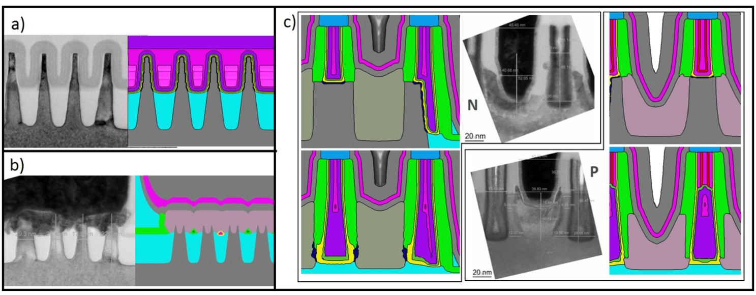
Fig. 1: Variation model calibration based on transmission electron microscope cross sections for (a) fin self-aligned double patterning, (b) source/drain epitaxial growth and contacts, and (c) gate-to-source/drains spacers. Source: Coventor/Lam Research
Power
Variation in power is particularly problematic with advanced nodes and packages because of the density, which makes it more difficult to dissipate heat. Variation can cause thermal hotspots in unexpected places because silicon conducts heat. So it can spread to other sections of a chip, making it difficult to pinpoint the source of the problem.
“One of the things a lot of people are running into with the newer nodes is lower operating voltages,” said Mike Kelly, vice president of advanced packaging development and integration at Amkor Technology. “There’s less margin for error. The IPs are operating with less tolerance for any variation — especially operating voltages. From a power delivery standpoint, getting local charge storage close to the die is becoming much more important at 5nm, and we’re anticipating much worse situations at 3nm. That variation is going to build up in the power supply. And then there’s mechanical and thermal variation.”
Power variation can occur for any number of reasons. It could be due to imperfections on a nanosheet FET, or it could be variation within a dielectric film, where one or two atoms of thickness can make a big difference in insulation properties. This is one of the benefits of modular, multi-die approaches, where advanced-node logic can be developed using very regular structures on a single die, separated from other functions that are developed using more mature processes.
“There’s quite a bit of research going on just on supplying power to the other side of a transistor because the power delivery takes up so many of the routing channels,” said Kelly. “Anytime you don’t have to go to the next node, you get an economic benefit because of the cost per wafer. And the older the node, the more tolerant it is to things like voltage variation. That’s why there’s so much interest in going heterogeneous. People are trying to segregate these issues. A long-reach SerDes I/O device doesn’t need 3nm processes.”
Variation in packages
The existing challenges for process and yield worsen at each new process node, as well. Defect density increased in the transition from 7nm to 5nm, which in turn lowered yield, according to multiple industry sources and presentations at industry conferences. No one is quite sure what the impact will be from moving to 3nm and 2nm, but there is almost universal agreement that all of these issues will be more difficult to deal with, which in turn will drive up prices.
This is why there is so much interest in chiplets. IDMs such as Intel, AMD and Marvell already are using chiplets internally. And Xilinx has been breaking apart its FPGAs into multiple chips connected through an interposer since 2011 as a way of improving yield. But this whole picture becomes more complicated as transistor and feature density increases, so the idea is to keep as much at mature nodes as possible, beef up the interconnect speed, and reduce the distance that signals need to travel.
While advanced packaging requires some sophisticated floor-planning in multiple dimensions, it can be used to minimize some variation effects. But not all packaging approaches deal with these problems equally.
“This is driving the whole evolution toward chiplets,” said Ingu Yin Chang, senior vice president of ASE Group. “People can use 3/2nm technologies in combination with more legacy solutions. That gives them the maximum feature set with the lowest possible cost. We’ve spent a lot of effort in trying to create a comprehensive toolbox to allow us to deal with variation because there is no one solution that can fit all. With chiplets, there are so many different ways that people are putting together 3D structures. TSMC has CoWoS (chip on wafer on substrate), InFO (integrated fan-out) and SoIC (system on integrated chip). Intel has its ODI (omni-directional interconnect) solution, which is a combination of different technologies including EMIB (embedded multi-die interconnect bridge). And recently we’ve seen Samsung’s X-Cube, which is an SRAM on top of a logic die. These are broad solutions to manage variation.”
On paper, all of this looks more attractive. But it’s far from simple. With Samsung’s X-Cube, for example, the SRAM is a significantly larger process than a 7nm logic chip. Integrating them on a single die is far more difficult than putting a high-speed interconnect between the two chips. Samsung uses through-silicon vias to connect the logic to the memory, with significantly shorter and much faster signal paths than would be possible on a large chip.
“The challenge is putting that all into an organic substrate,” said Chang. “Today, the tightest geometry we can use is a 2µm x 2µm line/space. That creates a whole bunch of issues with substrate limitations. Using RDL as a medium, or interconnect as a medium, or some sort of hybrid solution, is a way of trying to bridge that gap. As the pitch comes down, you are able to get more I/O and more power, but you don’t have structures to put that on. So not only do you have to deal with silicon at various technologies, but the substrate hasn’t quite caught up yet. The variation has created a gap. OSATs are trying to close that gap with solutions like fan-out.”
Tighter lines and spaces in all types of packaging means tighter tolerances, too, which again makes variation a much bigger deal.
“Increasingly complex advanced packaging techniques are requiring tighter process windows for many variation types,” said KLA’s Lenox. “A classic example would be how variation in micro-bump heights — before thermo-compression bonding — continues to need to be reduced as target micro-bump pitches decrease. But in addition, we are seeing advanced packaging driving entirely new integration schemes in order to meet variation and cleanliness requirements. For example, the use of plasma dicing for very clean, low-particle singulation is growing significantly. On the high-end IC substrates used in advanced packaging, the reduced tolerance to current process variation is driving higher levels of inspection, and in more cases the use of automated optical shaping (AOS) of shorts and opens to increase yield. In addition, impedance control to meet 5G RF requirements has clearly translated into increased requirements for CD and 3D metrology.”
Variation in materials
Materials play a big role in all processes, including the development of chips and packages. The tools to process those materials are also key. Both can contribute to systemic variation.
Consider the gap fill process in the fab, which is just one of many examples. To fill gaps, a system deposits materials in tiny gaps or trenches. However, this adds yet another possible source of variation, and one that operates well below the radar of most engineers.
“The goal of any dielectric gap-fill step is to complete the fill of the structures, without voids or seams,” said Aaron Fellis, corporate vice president and general manager of Dielectric ALD products at Lam Research. “The difficulty, of course, is that there is variability in those structures that was introduced in upstream processes. And today, we have the additional issue of filling incredibly small features that may also have incredibly large aspect ratios.”
The key with the most advanced nodes is to be able to control the fill process more tightly as it is happening, and to adjust to whatever variations are on a die or wafer in real time. This is required because the structures themselves are so fragile that correcting errors post-process can cause even more damage.
“You need to analyze the fill throughout the depth of the feature using various metrology approaches, and look at the fill properties themselves,” said Fellis. “This gap-fill oxide is used as an isolation layer, and you need consistent oxide properties at the top and the bottom. But the goal is general lifetime performance, so you need to know the films are stable.”
Variation adds some interesting twists here. For one thing, variation of any type — whether caused by manufacturing processes or differences in tools, or even between chambers in the same tool — can cause big problems in tight features. “ALD gives you the angstrom-level control needed to target those critical small features independently of larger features on the same level,” said Fellis.
Variation also affects other man-made materials in ways that are difficult to quantify. It may be the result of a single microscopic particle in a large 55-gallon drum that is used over the course of years, and creating that material may involve chemicals from parts of the supply chain that regard semiconductor companies as an insignificant part of their business.
“The specs and quality requirements are ridiculously high,” said Tom Brown, executive director of global corporate systems at Brewer Science. “The cost to get there for suppliers is daunting, and there is questionable return. So what we’ve done is take teachings from our customers and apply them across the supply chain. We’ve put together a cross-functional team to mitigate risk and looked at what we can build with our suppliers and how to compartmentalize processes to mitigate risk.”
This is a monumental task. “We have to test every raw material,” Brown said. “There’s also a lot of genealogy and traceability. But it still comes down to the supplier. Some of them don’t care. We’re at parts per trillion, and we’re looking at how to get to parts per quadrillion. In some cases that requires us to push our tools beyond the capability they were selling at. We’re looking for sub-parts per trillion ions, which is beyond the level you can buy today.”
Variation economics
All of this obviously has a big impact on cost. Managing cost always has been an issue with semiconductors, but it’s becoming a limiting factor in advanced-node chips. That cost is measured both in wafer yield and in the time it takes to complete the various process steps required for that wafer — or for different parts of a wafer.
At 7nm and 5nm, there can be hundreds or even thousands of process steps, which is why there is so much emphasis on the speed of the equipment at each step. Where individual steps take more time, equipment makers typically try to do multiple steps simultaneously.
But each process step also can contribute to variability, and that variability is incremental. While variability on one step may not itself cause a problem, in combination with other process steps it can push a chip, a package, or even an entire wafer out of spec. And with higher aspect ratios, as well as myriad advanced packaging options, keeping track of all of this becomes an immense challenge.
One approach is to do more data analysis from a higher level of abstraction, which is where AI/ML fits into the picture. AI can collect data and use it to predict where problems are occurring, or likely to occur, based upon large data sets.
“You’re constantly trying to get to a true, fundamental understanding of the process and the mechanism,” said David Fried, vice president of computational products at Lam. “We’re creating gigabytes of data per process run, but we’ve only started scratching the surface of how this data can be used. In the real world, you end up firefighting the most urgent yield limiters. Maybe we don’t have sensors, but we do have simple linear regression techniques to analyze data and failure mechanisms, and we can certainly keep going in that direction and continue using those techniques. However, maybe we also have 14 sensors providing feedback that correlates strongly to our underlying failure mechanisms. You can use this sensor data to build an arsenal of analytic techniques and go after each one of these failure mechanisms. The most difficult, complex, thorniest yield mechanisms are going to require the most advanced techniques, and we’re going to need to reach further into the data than we ever have before.”
That data also can point chipmakers in a different direction than they might originally have planned, including the type of package they ultimately choose.
“With the high-density fan-out, we’ve got a few more knobs to turn as far as dialing in heat, integrated memory, and also power distribution networking,” said Curtis Zwenger, vice president of advanced product development at Amkor. “We’ve had very good success converting both logic and RF devices to high-density fan-outs.”
One thing that would help significantly in all these cases is more automation and more visibility into these systems. Tools don’t exist to automate this process today. “A lot of the tools we have are layout tools,” said ASE’s Chang. “To deal with different types of variation, and process variation within a chip, you need to know more about the IP and the silicon.”
Where better equipment does exist, it’s expensive, and it requires additional equipment and domain expertise to be able to understand the data. “Traditional inspection is not good enough, whether that’s brightfield or darkfield,” said Damon Tsai, director of inspection product management at Onto Innovation. “You always need to use the light source on top of the wafer surface, at 0° or 90° angles, but they will only penetrate the first layer and into the next layer, and the bottom layer. And they also reflect a lot of noise. As you start to use a very high resolution rate, they will see even more noise.”
New bonding approaches add to complexity. At 3nm, for example, hybrid bonding begins to enter into the picture and costs for inspection increase further, although for different reasons.
“At that point, you will no longer use copper pillars,” Tsai said. “It will just be the bump pads to replace copper pillars. For bump pads, right now we’re seeing 5µm, and the roadmap for more advanced technology is down to 3µm and below. That will bring new inspection challenges because the hybrid bonding people are starting to talk about chip-to-wafer and wafer-to-wafer. And if you’re doing chip-to-wafer bonding, known good die becomes very important. You don’t want to bond the bad dies on top of the whole wafer. In the past, the inspection sampling rate was probably about two or four wafers per lot, but with hybrid bonding customers are telling us they want 100%.”
Conclusion
Variation is both a localized problem and a system-level issue. It affects everything from the front end to the back end of the manufacturing process, and the entire supply chain. It may cause a problem in some architectures and not in others. And when it does cause a problem, the root cause may be difficult to find. Heat can spread on silicon, and finding the cause is like looking for a needle in several billion haystacks.
The challenge will only grow, too, as more components are packaged together, and as logic continues to scale down into the angstrom range. What used to be a simple matter of compensation is now a complex set of interactions that can affect everything from performance to quality over time, and that complexity will continue to balloon as the industry begins to shift from billion-unit SoCs to off-the-shelf chiplets and more disaggregation and customization. Variation is spreading, and integrated tools and methodologies will be needed to address these issues.
Related
Making Random Variation Less Random
Limits on margin and a growing emphasis on reliability are changing the economics of unknowns.
Dealing With Sub-Threshold Variation
The value and challenges of circuits being not quite on or off.
Wrestling With Variation In Advanced Node Designs
Margin is no longer effective, so now the problem has to be solved on the design side.
Controlling Variability And Cost At 3nm And Beyond
Lam’s CTO talks about how more data, technology advances and new materials and manufacturing techniques will extend scaling in multiple directions.
Variation Issues Grow Wider And Deeper
New sources, safety-critical applications and tighter tolerances raise new questions both inside and outside the fab.

 |
|
 |
|
 |
 |
 | |
 |
 |
Leave a Reply