New architectures, packaging approaches gain ground as costs increase, but shrinking features continues to play a role.

The growing challenges of traditional chip scaling at advanced nodes are prompting the industry to take a harder look at different options for future devices.
Scaling is still on the list, with the industry laying plans for 5nm and beyond. But less conventional approaches are becoming more viable and gaining traction, as well, including advanced packaging and in-memory computing. Some options are already here, while others are still in R&D and require more funding to get off the ground. Some may never work.
Nevertheless, the industry is looking for solutions, whether that involves IC scaling or novel approaches.
Chip scaling is being pursued by several chipmakers and foundry customers. For this, chipmakers are ramping up 10nm/7nm, with 5nm and 3nm in R&D. But at each node, the costs are escalating, meaning that only a select few with deep pockets can afford to migrate to the next step. Plus, the benefits of scaling are shrinking at each node, and the traditional approach is no longer suitable for all devices.
Even Intel, which created Moore’s Law, is coming to grips with the issues and is re-thinking the way chips are developed amid the shift towards 5G, artificial intelligence and machine learning.
“In the previous generations, the answer has been that transistor density and Moore’s Law will play the lead role to solve computing problems,” said Raja Koduri, senior vice president of Core and Visual Computing at Intel. “But as the process node transitions have slowed from the pace of the previous decades, it is the essence of Moore’s Law that continues to provide new technologies and capabilities to meet the demands of modern computing. The message of Moore’s Law is about more than transistors alone, with the combination of transistors, architectural research, connectivity advancements, faster memory systems, and software working together to drive it forward.”
This is not to say Intel or others have stopped scaling. But in addition to monolithic device scaling, the industry is looking at new ways to move the ball forward. For example, a growing list of entities are throwing their weight behind the chiplets model. Intel and TSMC are the latest backers of chiplets.
“What we’ve done over the last 15 to 20 years is to let the leading edge—the fast-path computing part of whatever product you’re designing—push the technology, and everything else we want to integrate on that chip comes along with it,” said David Fried, CTO at Coventor, a Lam Research Company. “You can do you I/O circuits, your low-speed data path, memory, power conservation. Okay, it’s going to be in the advanced technology, but that’s not really why we did the advanced technology in the first place. We’re still doing something similar. A lot of these high-end applications are still driving the front-end of technology, but instead of just dragging along memory we’re going to heterogeneous integration. Instead of just dragging along the I/O or the analog part, we’re going to some 3D stacking to put those together. So everything is customized, but only because we’ve kind of stopped just dragging them along into the most advanced technology.”
In this changed environment, chipmakers and foundry customers must keep a close eye on the various manufacturing and related options to enable future devices. Some may use more than one option as there is no one technology that fits all applications. And, of course, not all will migrate to advanced nodes.
Among the leading options:
Going to gate-all-around
For more than half a century, the growth engine has revolved around Moore’s Law, the axiom that states transistor density would double every 18 to 24 months. Adhering to Moore’s Law, chipmakers introduced a new process in that time interval to lower the cost per transistor.
At each node, chipmakers scaled the transistor specs by 0.7X, enabling the industry to deliver a 40% performance boost for the same amount of power and a 50% reduction in area. That formula worked until 20nm, when traditional planar transistors ran out of steam due to technical issues. In response, Intel moved to finFETs at 22nm, followed by the foundries at 16nm/14nm. In finFETs, the control of the current is accomplished by implementing a gate on each of the three sides of a fin.
Before 14nm, there was a 30% improvement in price/performance at each node, according to analysts. From 14nm to 10nm, there is more than 20% improvement, and at less than 10nm there is more than 20%. At 3nm, there is about 20% improvement, analysts said.
However, the industry was forced to move from planar to finFETs at 20nm. The industry faced short channel effects and other issues at 20nm. In other words, finFETs solved those problems, but it’s debatable if you get the traditional scaling improvements at each node.
FinFETs do provide more performance with lower power, but it becomes more difficult to scale them at each node. As a result, the cadence for a fully scaled node has extended from 18 months to 2.5 years or longer. In addition, fewer foundry customers can afford to move to advanced nodes. IC design costs have jumped from $51.3 million for a 28nm planar device to $297.8 million for a 7nm chip and $542.2 million for 5nm, according to IBS.
“PPAC (power, performance, area, cost) scaling at the leading edge is getting more complex and costly,” said Yang Pan, corporate vice president of advanced technology development at Lam Research. “As process complexity increases, managing process-to-process interaction through advanced process control is a must to reduce variation.”
Over time, the market split into two camps. One involves IC suppliers that don’t require finFETs or can’t afford them. This includes analog, mixed-signal and RF, which use mature processes. That market is thriving.
For example, several foundries offer finFET processes. Yet, demand is robust for mature processes at 40nm and above. “UMC is experiencing high demand from mature 12-inch processes,” said Jason Wang, co-president of UMC. “With new applications in 5G, IoT, automotive and AI requiring these technologies, we anticipate the market conditions driving this demand to remain strong for the foreseeable future.”
Even 200mm fab capacity and chips are still in high demand. “For the 8-inch, we have to remain optimistic and cautious about the 8-inch outlook. We have pretty good confidence that we will remain fully loaded in Q4 2018,” Wang said in a recent conference call.
The second camp involves companies that continue to scale and require high-performance chips. “Moore’s Law is definitely slowing down, but I’m confident there will be continued innovation everywhere to keep it going for a while,” said Aki Fujimura, chief executive of D2S. “Regardless, there’s no question there is a need for more compute power. There was some talk of how we can no longer use more compute power perhaps 10 years ago. There’s no more talk about that now.”
For years, IC scaling has been the main way to boost transistor density and enable high-performance chips. Today, 7nm is the most advanced process. By most accounts, 7nm is expected to be a long-running node, as it provides enough PPAC for most apps.
Still, TSMC plans to extend the finFET to 5nm, which is slated for 2020. But finFETs will likely run out of steam at 5nm, meaning the industry will require a new transistor type at or around 3nm.
Moving to a new transistor type isn’t simple. It requires new tools, materials and integration schemes. Plus, the IC design costs will be astronomical at 3nm, so the big question is whether anybody will migrate to this node.
“Initially, there will be the usual suspects working with 3nm, such as Nvidia, Xilinx, Apple and Samsung,” said Joanne Itow, an analyst with Semico Research. “Once they get all the kinks worked out, you’ll see Qualcomm, MediaTek, AMD, Intel (Altera) and others jumping on board.”
The industry has been working on next-generation transistors in R&D, and for 3nm it has narrowed the field to two technologies, nanosheet and nanowire FETs. Both are classified as gate-all-around technologies. They implement a gate on four sides of the structure, enabling more control of the current.
The nanosheet FET is the current favorite. It has a wider channel than the nanowire, enabling more drive current. Plus, the nanosheet is an evolutionary step from a finFET, meaning it uses many of the same process steps. In a nanosheet, a finFET is placed on its side and is then divided into separate horizontal pieces, which make up the channels. A gate wraps around each channel.
In 2017, Samsung introduced what it calls a Multi Bridge Channel FET (MBCFET), which is a nanosheet FET. Targeted for 3nm, Samsung’s MBCFET is slated for production in 2020. Intel and TSMC haven’t announced their plans beyond finFETs.
At the recent IEDM conference, Samsung presented its first results with MBCFET, saying it has developed a functional SRAM device. “Three representative superior characteristics of MBCFET compared to finFET have been demonstrated — better gate control with a 65mV/decade sub-threshold swing at a short gate length; higher DC performance with a larger effective channel width at a reference footprint; and design flexibility with variable nanosheet widths,” said Geumjong Bae, a researcher at Samsung.
A nanosheet FET enables the industry to vary the width of the channels or sheets in devices. For example, a nanosheet FET with a wider sheet provides more drive current and performance. A narrow nanosheet has less drive current, but it takes up less area.
All told, nanosheet FETs enable the industry to scale a device when finFETs hit the wall. But nanosheets provide only marginal gate-pitch scaling benefits. Design costs are the other big issue.
What is monolithic 3D?
The industry has been working on alternatives, as well, including monolithic 3D—sometimes called 3D sequential integration.
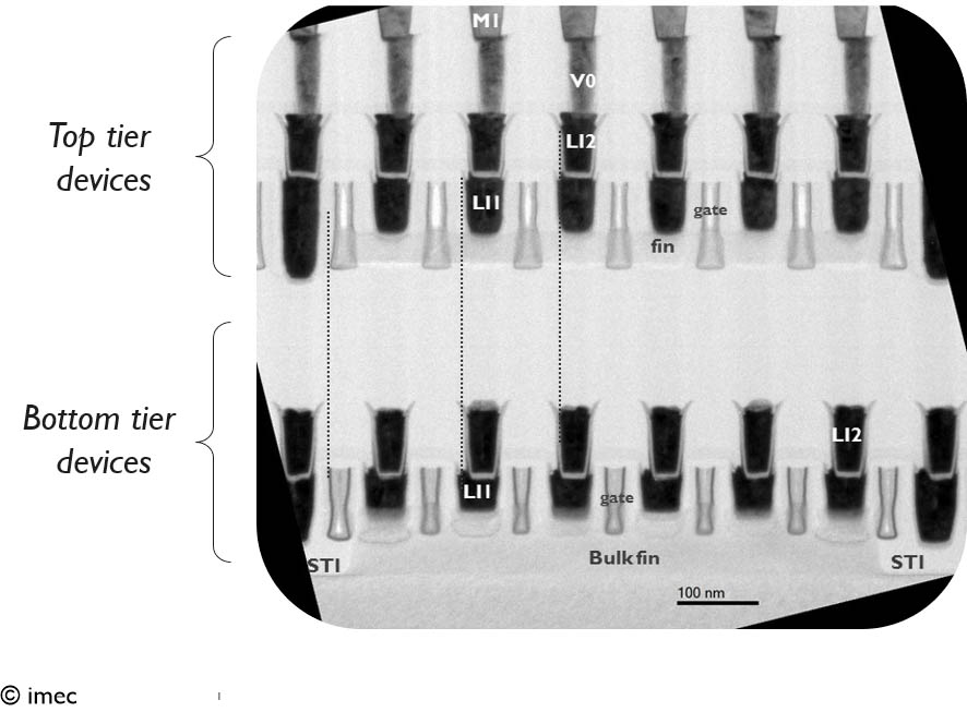
In simple terms, you develop a layer of transistors on one substrate. The transistor type depends on the application, but you could use analog, logic or memory. Then, you develop another layer of transistors on another substrate. The two layers are bonded and connected using tiny interconnects, and the end result is a 3D monolithic device. The technology has demonstrated up to a 50% area reduction in devices, according to Imec.
DARPA, Imec, Leti and others are pursuing the technology in R&D, although it’s unclear when it will appear in the market because there are several challenges to solve. For instance, the top layer requires various process steps with temperatures around 500°C. Otherwise, the top layer can degrade the bottom tier. So the industry requires tools that work at lower temperatures, which has been the primary roadblock.
There are reports of progress. For example, using a 3D sequential process with temperatures at 520°C, Imec stacked two layers of finFETs on top of each other. The finFETs have a 45nm pitch and 110nm gate pitch.

Fig. 1: Stacking finFETs on finFETs Source: Imec
In sequential processing, you have a substrate, based on either bulk CMOS or silicon-on-insulator (SOI) technology. Then, you build two tiers (bottom and top) on the substrate. In the flow, you first build the bottom tier with a layer of transistors.
“You build your first layer of the device. We did it with bulk finFET, but it could be any technology,” said Anne Vandooren, principal member of the technical staff at Imec.
Then, a level of interconnects are processed on that layer. The next step is to fabricate the top with a layer of transistors. The bottom and top layers are bonded.
This isn’t limited to finFETs. “It really depends on the application. It can be a CMOS logic cell on a CMOS logic cell. Or it could be another application like RF on logic, sensor on logic, memory on logic, or logic on memory,” Vandooren said.
Leti, meanwhile, has been working on a similar technology, and has recently developed some new capabilities. First, Leti has demonstrated a low-resistance polysilicon gate for the top transistors. The layer was processed using a nanosecond laser anneal tool, which works at higher temperatures without impacting the bottom level. The R&D organization also has developed an epi process at 500°C. It has developed other processes, as well.
“This integration scheme offers a wide spectrum of applications, including for example: 1) increasing integration density beyond device scaling; 2) enabling neuromorphic integration where RRAM is placed between top and bottom tiers; and 3) enabling low-cost heterogeneous integration for smart sensing arrays,” said Maud Vinet, advanced CMOS laboratory manager at Leti.
Processing in memory
There are other approaches, as well, namely using a memory-centric technology. Today’s memory hierarchy is straightforward. SRAM is integrated into the processor for cache. DRAM is used for main memory. And disk drives and NAND-based solid-state storage drives (SSDs) are used for storage.
In systems, data moves between the memory and a processor. But at times this exchange causes latency and power consumption, which is sometimes referred to as the memory wall.
DRAM is one of the culprits. The data rates for DRAM have fallen behind in terms of bandwidth.
The industry has been working to resolve this problem for years. The latest solutions involve two technologies—near-memory computing and in-memory computing. “The growing trend of near-memory computing and in-memory computing will drive new architectures that are integrating logic (digital and analog) and new memories,” Lam’s Pan said.
Near-memory computing isn’t new. It involves integrating high-bandwidth memory (HBM) in a package, enabling faster data access and lower power consumption. For example, in a 2.5D package, a vendor could incorporate a graphics processor and HBM, which stacks DRAM dies on top of each other to enable more I/Os.
In-memory computing, sometimes called processing in-memory, also is emerging. This concept means different things to different people. In some circles, in-memory computing involves a process in which the computations are performed within the memory and/or at the location of the data storage.
The idea has been around for years, but the early efforts fell short. Today, chipmakers, startups, R&D organizations and universities are working on the technology and making progress.
“There are products coming out in that direction. In-memory computing is happening now using existing memory technology. The products are being built specifically for those applications. That will drive more segmentation in memory applications,” said Gill Lee, managing director of memory technology at Applied Materials.
For example, startup Mythic recently introduced a matrix multiply memory architecture. It performs the computations inside the memory cells using analog currents and flash memory.
“Mythic does this in a 40nm process. Effectively, Mythic has turned back the clock on process scaling,” said Dave Fick, CTO of Mythic, in a blog. “While other system designers are struggling to get from 7nm to 5nm, Mythic will be scaling to 28nm.”
Mythic and others are using the technology to drive neural networks. In neural networks, a system crunches data and identifies patterns. It matches certain patterns and learns which of those attributes are important.
A neural network consists of an input layer, a hidden layer, and an output layer. Data is fed into the input layer and then processed in the hidden layer with a set of coefficients. This either amplifies or dampens the input using a weighted system, “thereby assigning significance to inputs for the task the algorithm is trying to learn,” according to AI startup Skymind.
The problem is that the data exchange is sometimes slow and consumes power. “To overcome this challenge, in-memory computing, where computing is done at the location of the data storage, has been proposed to accelerate the computation,” said Xiaoyu Sun, a Ph.D. student from Arizona State University and lead author in a paper at IEDM. The paper was co-authored by the University of Notre Dame and the Georgia Institute of Technology. (Sun has transferred to Georgia Tech.)
There are some limitations using existing memories, however. “The in-situ training accuracy suffers from unacceptable degradation due to undesired weight-update asymmetry/nonlinearity and limited bit precision,” Sun said.
Instead of using existing memory, ASU, Notre Dame and Georgia Tech are exploring the use of a 2T-1C ferroelectric FET (FeFET) memory technology. “We propose a novel hybrid approach where we use a modulated ‘volatile’ gate voltage of a FeFET to represent the least significant bits for symmetric/linear update during training only, and the use of nonvolatile polarization states of the FeFET to hold the information of most significant bits for inference,” Sun said.
Others are also working on the technology. For example, Leti is developing in-memory computing using RRAM, while Samsung is utilizing MRAM. It’s too soon to tell which technology will prevail.
“You will get different answers about the definition of in-memory computing, depending on who you ask,” Applied’s Lee said. “Although memory-centric computing is still in the early stages, what is evident is how the traditional borders of memory tasks are becoming blurred.”
Another in-memory computing technology type is called neuromorphic computing. In simple terms, neuromorphic computing enables massively parallel analog computing for deep learning apps. “Neuromorphic memory is more long term. The candidates are more like ReRAM and new memories, especially filament-type ReRAM. Other types of memories, including phase-change memory, can be used in neuromorphic computing,” Lee said.
Chiplets mania
Advanced packaging has been making gains in the market as an alternative to chip scaling. Different approaches have been used in limited form for decades in niche applications. Cost has been one of the main challenges here, but that could change as the industry marches toward heterogeneous integration, which involves putting multiple chips in an IC package.
“An evolution in packaging technology is being driven by a slowdown of Moore’s law,” said Pieter Vandewalle, general manager of the ICOS division at KLA-Tencor. “This is driving IC designers to work on both chip and package design to optimize the electrical and thermal behavior, and ultimately define the performance of the total package.”
There are several ways to implement multi-die packages, such as 2.5D/3D and fan-out. In one example, Amkor and GlobalFoundries recently presented a paper on a 22nm FD-SOI device, which is housed in an advanced wafer-level package. The companies devised a test vehicle, and the goal was to study the chip-board interaction of the package.
“Recently, wafer-level packaging has been in high demand, especially in mobile device applications as a path to enable miniaturization while maintaining good electrical performance,” said Jae Kyu Cho, a packaging engineer at GlobalFoundries, during a recent event. “The 22nm FD-SOI technology platform is an advanced silicon node for energy-efficient applications that deliver finFET-like performance. Combining both technologies will make it more attractive for various markets, such as 5G mmWave, IoT, wearables and automotive.”
The latest craze is chiplets. In chiplets, the idea of putting together different modules like LEGOs has been talked about for years, but few have implemented it.
Now, momentum is building for chiplets for various apps. For example, there is a surge for compute-intensive specialized applications, such as machine learning. This is driving the need for domain-specific architectures like hardware accelerators.
Needless to say, these devices must be economically feasible to design and fabricate. That’s where chiplets fit in. “To meet current and future growth demands, providers need a more efficient approach to satisfy the needs of a wide range of data center applications,” said Kevin O’Buckley, general manager at Avera Semiconductor, the ASIC spin-off from GlobalFoundries.
Chiplets are just one option on the table. Chip scaling and other approaches also remain in play. It’s likely that the industry will need more than one option.
As before, it boils down to cost, performance and power. The industry is just beginning to sort out the issues. It will take time before the dust settles.
Related Stories
 |
 |
 |
|
 |
 |
 |  |
Thank you. Its always inspiring to read your articles. This article points to starting a new renaissance in order to direct the path finding for the new technology.
We cannot recycle 50 year old concepts over and over to gate/negate the scaling factor.